 |
|
|
|
|
|
|
|
|
|
|
|
|
|
|
|
|
|
|
|
|
|
|
|
|
|
|
|
|
|
|
|
|
|
|
|
|
|
|
|
|
|
|
|
|
|
|
|
|
|
|
|
|
|
|
|
|
|
|
|
|
|
|
|
|
|
|
|
|
|
|
|
|
|
|
|
|
|
|
|
|
|
|
|
|
|
|
|
|
|
|
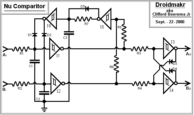
| Nu Comparator |
|
|
| This circuit grew out of my desire to give my robot the ability to compare the outputs of two sensors, to find which is higher and by how much. I wanted the robot to ignore the sensors as long as they were approximately equal, and react to them only when they were different. |
|
|
|
There is nothing really new here. Much of what is in this article grew out of other projects I have worked on, or was inspired by the work of others. In fact the idea for the Nu Comparator itself was inspired by Wilf's Aqua Detector, which can be found in the Alt-BEAM archive. But I thought there was enough interesting material to justify putting it together and sharing it with the group. |
|
|
|
A quick look at the schematic should make it clear why I call it a Nu Comparator. The concept is somewhat similar to the Pulse Width Key circuit in that the input and the reset portions, are Nu's (Neural Neurons). |
|
|
 |
|
|
Figure 1 |
|
|
Parts List A |
|
|
|
|
|
|
R1, R2 - 1K to 10Meg |
|
|
|
R3. R4, R5, R6 - 1Meg |
|
|
|
R7 - 2.2K |
|
|
|
C1, C2, C3 - .01uf |
|
|
|
I 1 to I 6 - 74 ** 14 |
|
|
|
The inputs |
|
|
|
The circuit is built around a 74 **14 hex inverting schmitt trigger. As stated, each input is a basic Neural Neuron (Nu). The better the components of the two input Nu?s are matched the better the circuit will function. |
|
|
|
C1 and C2 of the two input Nu's are both .1uf capacitors. For R1 and R2, I have tried several values ranging from 1K to 10Meg. The larger values produce longer output pulses but also tend to make the comparitor slower to respond. They also require a larger change at the inputs before they will react. Smaller value resistors produce smaller pulses, but also result in a faster reaction time to smaller differences in the inputs. |
|
|
|
The Outputs |
|
|
|
There are two outputs labeled Ao and Bo. Output Ao will generate high pulses whenever input Ai is higher than Input Bi, otherwise it will be low. Of course if input Bi is higher than input Ai, then the high pulses will appear at output Bo instead. The width of these pulse is determined by difference between the time it takes for the two Nu's to cycle in response to the voltages applied to their inputs. I the inputs are close to equal, then both outputs wil be low. |
|
|
|
The current limiting resistors R3 and R4 are used to connect the outputs of inverters I1 and I2 to the inputs of I3 and I4 and allow the output inverters to be cross coupled. A high on the output of I3 passes through D3 to the input of I4. A high on the output of I4 passes through D4 to the input of I3.This holds the output of I3 low. In this way only one output can be high at a time. This reduces the possibility of even a small spike from being produced on the inactive output during the moment before the circuit is reset. |
|
|
| Resetting |
|
|
|
R5 and R6 (both 1Meg) along with I5 form an interesting "X-Nand" kind of gate who's output goes high only when Nu1 and Nu2 have timed out and the outputs of both are low. It's output will go low when Nu1 and Nu2 are reset and their outputs both go high. It will hold the output state it is in if the outputs of the two input Nu's are in opposite states. See the chart in the section on using a 74HCT14 chip. |
|
|
|
Wilf Rigter has written about this type of arrangement, which he refers to as majority logic. In response to a short note on the "X-Nand" that I posted to the group, Wilf posted an address for the Nu Pages on Chui's site . There is a piece he had written on the subject. If you haven't already visited Chui's Site, or read any of Wilf's articles that he has collected there, I highly recommend that you do so. |
|
|
|
Anyway, R7, C3, D5 and inverter I6 form a third Nu who's input is tied to the output of inverter I5. When Nu1 and Nu2 have both timed out, their outputs will both be low, so the output of I5 will go high. D5 allows the high output of I5 to pass directly to C3 and the input of I6. This causes the output of I6 to go low. |
|
|
|
A low at the output of I6 passes through D1 and D2 to reset Nu1 and Nu2. When the outputs of Nu1 and Nu2 both return to a high state, the output of I5 returns to a low state. This begins to discharge C3 through R7. The output of I6 will remain low until the charge on C3 drops below the low going threshold of I6. This short delay, will all but guarantee that C1 and C2 are fully discharged, so that Nu1 and Nu2 both start out at the same point. |
|
|
|
When the reset process is complete, the Ao, and Bo outputs will again be low and the process will begin again. In this way, a series of pulses will continually be produced until Ai and Bi are both approximately equal. |
|
|
|
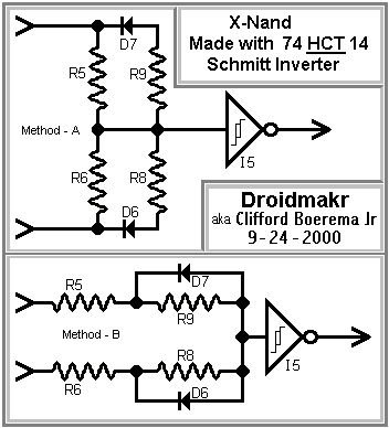
Using A 74HTC14 |
|
|
|
If you purchased your chip off the rack from Radio Shack, it is most likely a 74HTC14. This presents a bit of a problem in the reset portion of the circuit. Unfortunately, due to the asymmetry of this chips inputs we cannot get away with using two resistors to hold the input of the inverter between the high going and low going thresholds. But there is a way to use this chip. In fact, as shown in the schematics below, there are two arrangements that will work. |
|
|
|
Parts List B |
|
 |
|
|
|
|
- Method - A - - Method - B - |
|
|
|
R5, R6 - 330K - 220K |
|
|
|
R8, R9 - 100K - Same |
|
|
|
D6, D7 - Any common type - Same |
|
|
|
I5 - 1/6 of 74 HTC 14 - Same |
|
|
|
 |
|
|
|
Figure 2 |
|
|
|
|
The trick is to use a couple of diodes, so that the resistance is higher if the inverter tied to the input is high, and lower if it is low. In this way, if the outputs of Inverters I1 and I2 are in opposite states the voltage at the input of I3 will fall between it's high and low going thresholds. Which method you choose is up to you. |
|
|
|
In both methods R8 and R9 are 100K. However in method - A, R5 and R6 are 330K and in method - B, they are 220K. These values seemed to work well for me. |
|
|
|
Testing |
|
|
|
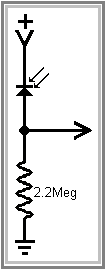
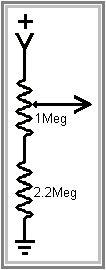
I first tested the circuit using 10K resistors for R1 and R2 and connecting a separate 1Meg pot and 2.2Meg resistor to each of the inputs. The resistor was tied between the pot and ground (negetive). I then adjusted each separately and observed the results. There was a small dead band but generally the circuit seemed to work pretty well. I then connected a photo diode and resistor arranged as a voltage divider in place of one of the pots and tried it. I set the pot to a point about in the center of it's sweep and used a small flashlight to apply different levels of light to the photodiode. Again I was pleased with the results. |
|
|
|
 |
|
|
 |
|
|
|
|
|
|
Figure 3 |
|
Figure 4 |
|
|
|
Then it hit me |
|
|
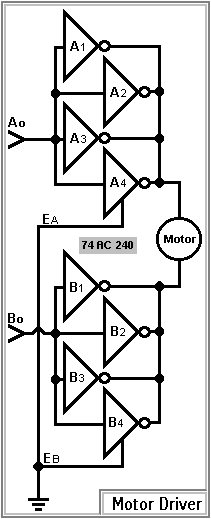
| Hey, this thing has two output lines that when active are in opposite states. I could use it to control a motor directly. I know I know, Uh-Duhh. But I originally was thinking about using it to influence the behavior of a controller. I wasn't even thinking about direct control of a motor. |
|
|
|
Anyway, I gave it a try. I used a 74AC240 as a motor driver to provide the needed current. The A inverters were tied together in parallel as were the B inverters. Ao was tied to the input of the A inverters and Bo was tied to the input of the B inverters. Both enable pins of the 240 were tied to the ground. The motor leads were then connected to the output side of the A and B inverters of the 240 chip. |
|
|
|
 |
|
|
|
Figure 5 |
|
|
|
|
|
I then connected a photodiode and resistor to each input. Both photodiodes were mounted to a gear motor I had on hand. It tracked the flashlight quite nicely. The dead band area did not appear to create any problems. Of course, it is not as efficient a Head circuit as Wilf's Power Smart Head, so I do not recommend it for that purpose. |
|
|
|
After that, I removed the photodiodes and put the pots back in place. I then mounted one of the pots, along with a piece of stiff wire to act as a pointer, to the shaft of the motor. I could then adjust the angle that the piece of wire was pointing by adjusting the other pot. Again the dead band area did not seem to have a major effect on the performance of the circuit. This might be useable as a kind of servo controller. It could be used for controlling the angle of a motor driven leg joint. |
|
|
|
Since the pulses get shorter as the inputs become more equal, the motor slows as it approaches it's new position. This reduces the likelihood of overshoot. Once again I was pleased with the way the circuit performed. |
|
|
|
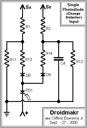
Detecting Sensor Change |
|
|
|
I then decided to see if I could use this circuit to detect changes in a sensor. Unfortunately, an accidental short circuit smoked my last 74HC14 so this bit of work had to be done with a 74HCT14. This may or may not have an influence on the results. |
|
|
|
I connected a single photodiode to both inputs through a pair of identical "T" type resistor networks. R1 and R2 are the the R1 and R2 of the main circuit and in this case are 100K. |
|
|
|
 |
|
|
|
Parts List C |
|
|
|
|
|
R1, R2 - 100K (these are part of the main circuit) |
|
|
|
|
|
R11, R12 - 150K |
|
|
|
|
|
R13, R14 -15K |
|
|
|
|
|
C4 - 1 to 5uf |
|
|
|
|
|
D8, D9 - Any common type |
|
|
|
|
|
PD1 - Photodiode |
|
|
|
|
|
Figure 6 |
|
|
|
|
|
I also tied a 1uf capacitor between the common connection point of the resistor "T" on one side of the circuit and ground, as shown in the schematic. The capacitor creates a short delay in any change in Sensor output SB.Changes on SA are not delayed but directly reflect changes in the light detected by the photodoide P1. It took a bit of tweeking to find the values that worked best for the capacitor and resistors, but the ones listed seem to work. |
|
|
|
I again used a small flashlight to test the response of the circuit, to changes in the amount of light falling onto the photodiode. Although the circuit does respond to changes in the input, it has to be a rather quick and good size change to trigger a response. Increasing the value of C4 helps a little but it does not entirely solve the problem. It also has the side effect of slowing the response time of the circuit. This may be related in part, to the dead band of the comparator circuit itself. |
|
|
|
I intend to keep experimenting with this idea because I think that if I can get the circuit to respond to smaller, and if possible, slower changes, it could be very useful. Any suggestions would be appreciated. |
|
|
|
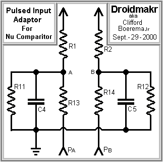
Pulsed Inputs |
|
|
|
Lastly, I thought I try comparing two different strings of pulses. I used a similar arrangement to the change detector idea. It of course has two inputs and a capacitor on each side. Using 3.3uf capacitors for C4 and C5 worked fairly well. The input that had the highest ratio of high pulses to low, would produce a high output. However, if the ratios were close to equal, the outputs would tend oscillate back and forth. |
|
|
|
 |
|
|
|
Parts List D |
|
|
|
|
|
R1, R2 - 100K (these are part of the main circuit) |
|
|
|
|
|
R11, R12 - 150K |
|
|
|
|
|
R13, R14 -15K |
|
|
|
|
|
C4, C5 - 3.3uf |
|
|
|
|
|
D8, D9 - Any common type |
|
|
|
|
|
Figure 7 |
|
|
|
|
|
In Conclusion |
|
|
|
Overall, I have enjoyed experimenting with this circuit and I believe it may prove to be a potentially useful and versatile concept. I'm sure that there is a lot of room for improvement in the basic circuit, so I intend to keep experimenting with it. Again, any suggestions will be greatly appreciated. And if you decide to experiment with it, Drop me an E-Mail and let me know how it worked out for you and what you think. |
|
|
|
So long, |
|
|
|
 |
|
|
|
|
 |
|
|
Droidmakr |
|
|
|
|
|
|
|
Sept. - 30 - 2000 |
|
|
|
|
|
|
|
|
|
 |
|
|
|
|
|
|