
GENERAL DESCRIPTION
The Z86E04/E08 One-Time-Programmable (OTP) microcontrollers are pin compatible to the masked ROM Z86C04/C08 devices. OTPs are designed to verify software and hardware functionality through quick pilot production for debugging and prototyping without committing to a masked ROM device. However, Zilog's OTP manufacturing capability allows high-volume production of these devices.
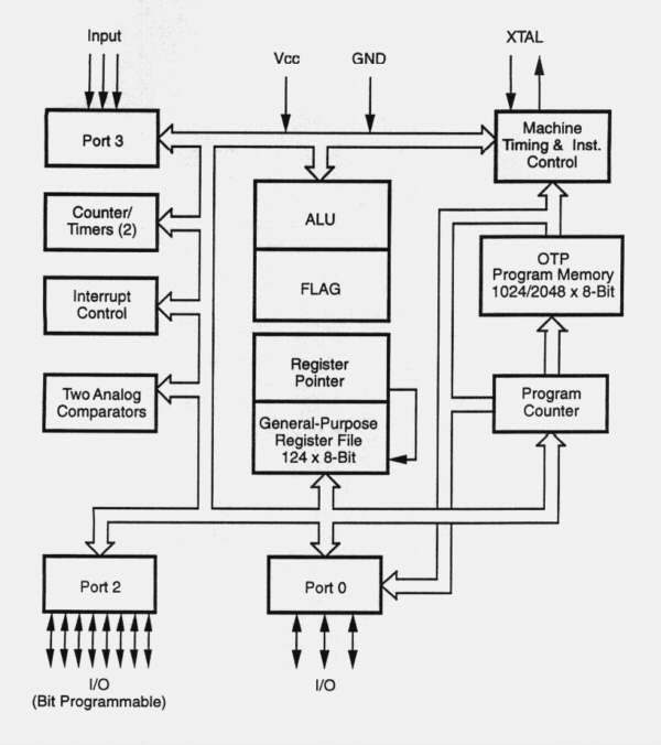
The Z86E04/08 are full-featured members of the Z8® microcontroller family offering a unique register-to-register architecture that avoids accumulator bottlenecks and is more code efficient than RISC processors.
The Z86E04/E08 are designed for use in a wide variety of embedded control applications such as keyboards, telephone answering machines, IR remotes, appliances, security systems, electronic games, and automotive modules.
For applications demanding powerful I/O capabilities, the Z86E04/E08 devices feature 14 pins dedicated to input and output. These lines are grouped into three ports, and are configurable under software control to provide I/O, timing, and status signals.
Two on-chip counter/timers, with a large number of user-selectable modes, are available to relieve the system of administering real-time tasks, such as counting/timing and I/O datacommunications.
The Z86E04/E08 have two on-board comparators with a common reference that implements analog functions such as A/D conversion.
Six different internal or external interrupt sources are maskable and prioritized in which a vectored address is provided for efficient interrupt sub-routine handling and multitasking functions.
Z86E04/E08 Functional Block Diagram
The Z86E30/E31 One-Time-Programmable (OTP) microcontrollers are pin
compatible to the masked ROM Z86C30/C31 devices. OTPs are designed to
The Z86E30/E31 are full-featured members of the Z8® microcontroller
family offering a unique register-to-register architecture that avoids
accumulator bottlenecks and is more code efficient than RISC processors.
The Z86E30/E31 are designed to be used in a wide variety of embedded
control applications, such as keyboards, telephone answering machines,
IR remotes, appliances, security systems, electronic games, and automotive
modules.
For applications demanding powerful I/O capabilities, the Z86E30/E31
devices feature 24 pins dedicated to input and output. These lines are
grouped into three ports, and are configurable under software control
to provide I/O, timing, and status signals.
Two on-chip counter/timers, with a large number of user-selectable modes,
are available to relieve the system of administering real-time tasks, such
as counting/timing and
I/O datacommunications.
The Z86E30/E31 have two on-board comparators with a common reference
that implement analog functions such as A/D conversion.
Six different internal or external interrupt sources are maskable and
prioritized in which a vectored address is provided for efficient interrupt
sub-routine handling and mulitasking functions.
By means of an expanded register file, the designer has access to three
additional system control registers which provide extra peripheral devices,
I/O ports, and register addresses. (See Functional Block Diagram).
Z86E30/E31 Functional Block Diagram.
Z86E04/E08 Pin Description:
                    _________    _________
                  _|         \__/         |_
        <--> P24 |_|1                   18|_| P23 <-->
                  _|                      |_
        <--> P25 |_|2                   17|_| P22 <-->
                  _|                      |_
        <--> P26 |_|3                   16|_| P21 <-->
                  _|        Z86E04        |_
        <--> P27 |_|4       Z86E08      15|_| P20 <-->
                  _|                      |_
             VCC |_|5                   14|_| GND
                  _|                      |_
       <-- XTAL2 |_|6                   13|_| P02 <-->
                  _|                      |_
       --> XTAL1 |_|7                   12|_| P01 <-->
                  _|                      |_
         --> P31 |_|8                   11|_| P00 <-->
                  _|                      |_
         --> P32 |_|9                   10|_| P33 <--
                   |______________________|
Z86E30/31
GENERAL DESCRIPTION

Z86E30/E31 Pin Description:
                    _________    _________
                  _|         \__/         |_
        <--> P25 |_|1                   28|_| P24 <-->
                  _|                      |_
        <--> P26 |_|2                   27|_| P23 <-->
                  _|                      |_
        <--> P27 |_|3     EPROM/OTP:    26|_| P22 <-->
                  _|        Z86E30        |_
        <--> P04 |_|4       Z86E31      25|_| P21 <-->
                  _|      MASK:           |_
        <--> P05 |_|5       Z86C30      24|_| P20 <-->
                  _|        Z86C31        |_
        <--> P06 |_|6                   23|_| P03 <-->
                  _|                      |_
        <--> P07 |_|7                   22|_| GND
                  _|                      |_
         +5V VCC |_|8                   21|_| P02 <-->
                  _|                      |_
       <-- XTAL2 |_|9                   20|_| P01 <-->
                  _|                      |_
       --> XTAL1 |_|10                  19|_| P00 <-->
                  _|                      |_
         --> P31 |_|11                  18|_| P30 <--
                  _|                      |_
         --> P32 |_|12                  17|_| P36 -->
                  _|                      |_
         --> P33 |_|13                  16|_| P37 -->
                  _|                      |_
         <-- P34 |_|14                  15|_| P35 -->
                   |______________________|
![]() Get your own Free Home Page
Get your own Free Home Page