| View Page Stats |
|
1. Introduction
1.1 History
In 1952 Radushkevich and Lukyanovich published clear images of 50 nanometer diameter tubes made of carbon in the Russian Journal of Physical Chemistry. This discovery was largely unnoticed, the article was published in the Russian language, and Western scientists' access to Russian press was limited during the Cold War. It is likely that carbon nanotubes were produced before this date, but the invention of the transmission electron microscope allowed the direct visualization of these structures. Since independent discoveries by Bethune at IBM and Iijima at NEC of single-wall carbon nanotubes, carbon nanotubes have been investigated by many researchers all over the world. Their large length (up to several microns) and small diameter (a few nanometres) result in a large aspect ratio. They can be seen as the nearly one-dimensional form of fullerenes. Therefore, these materials are expected to possess additional interesting electronic, mechanic and molecular properties. Especially in the beginning, all theoretical studies on carbon nanotubes focused on the influence of the nearly one-dimensional structure on molecular and electronic properties. Because of their many exceptional properties, which span the spectrum from mechanical and chemical robustness to novel electronic transport properties. Their physics, chemistry and perspectives for applications are very challenging
1.2 Types of carbon nanotubes
Many exotic structures of fullerenes exist .Regular
spheres, cones, tubes and also more complicated and strange shapes. Here this
paper will describe some of the most important and best-known structures.
·
Single-walled
Single-walled nanotubes (SWNT) have a diameter of close to 1 nanometer, with a tube length that can be many thousands of times larger than diameter. Single-walled nanotubes with length up to orders of centimeters have been produced as reported by Zhu, et al. in 2002. The structure of a SWNT can be conceptualized by wrapping a one-atom-thick layer of graphite called graphene into a seamless cylinder. The way of wrapping the graphene sheet is represented by a pair of indices (n,m) called the chiral vector. The integers n and m denote the number of unit vectors along two directions in the honeycomb crystal lattice of graphene. If m=0, the nanotubes are called "zigzag". If n=m, the nanotubes are called "armchair". Otherwise, they are called "chiral". Nanotubes generally have a length to diameter ratio of about 1000 so they can be considered as nearly one-dimensional structures.

Fig 1-1. A vector Ch
describes how to roll up the graphene sheet to make SWNT . a1 &
a2 are unit vectors in real space.
·
Multi-walled
Multi Walled Nanotubes (MWNT) can be considered as a
collection of concentric SWNTs with different diameters. The length and diameter
of these structures differ a lot from those of SWNTs and, of course, their
properties are also very different.There
are two models which can be used to describe the structures of MWNTs. In the Russian Doll model, sheets of graphite
are arranged in concentric cylinders, eg a single-walled nanotube (SWNT) within
a larger single-walled nanotube. In the Parchment
model, a single sheet of graphite is rolled in around itself, resembling a
scroll of parchment or a rolled up newspaper. The interlayer distance is close
to the distance between graphene layers in graphite.
Fig 1-2 :(top) cross-section of a MWNT, (bottom) 3D image of a MWNT.


1.3 Properties of carbon
nanotubes Density-CNTs
have a low density for a solid of 1.3-1.4 g/m³.
Chemical reactivity-As compared with a graphene sheet, reactivity
of CNTs is enhanced as a direct result of the curvature of the CNT surface. Carbon
nanotube reactivity is directly related to an increased curvature. For the same
reason, a smaller nanotube diameter results in increased reactivity.
 Mechanical
Strength-It is becoming clear from recent experiments that CNTs are
fulfilling their promise to be the ultimate high strength fibres for use in
materials applications. CNTs are one of the strongest materials known in terms
of tensile strength and elastic modulus .A high carbon steel sample has
strength of approximately 1.2 GPa ,whereas a MWNTs have a tensile strength of 63 Gpa. CNTs are not nearly as strong under
compression. Because of their hollow structure and high aspect ratio, they tend
to undergo buckling when placed under compressive, torsional or bending stress.
Mechanical
Strength-It is becoming clear from recent experiments that CNTs are
fulfilling their promise to be the ultimate high strength fibres for use in
materials applications. CNTs are one of the strongest materials known in terms
of tensile strength and elastic modulus .A high carbon steel sample has
strength of approximately 1.2 GPa ,whereas a MWNTs have a tensile strength of 63 Gpa. CNTs are not nearly as strong under
compression. Because of their hollow structure and high aspect ratio, they tend
to undergo buckling when placed under compressive, torsional or bending stress.
Kinetic-Graphite sheets slide past each other with relatively little friction, and it has been predicted that MWNTs could also readily slide past each other. The inner bundle could be slided out of the outer bundles & by predictions van-der-Waals forces rapidly retract it back into the bundle.
Electrical-CNTs, especially SWNT are considered as prototypes of 1D conductors.The electronic properties of one-dimensional conductors have generated a lot of interest both experimentally and theoretically. The reason for this excitement lies in the very rich phase diagram of a 1D conductor and the prediction that in a 1D system Coulomb interactions should lead to a strongly correlated electron gas, called a Luttinger liquid (LL), instead of the usual quasi-particle picture described by a Fermi-liquid. The current in MWNTs, contacted by metallic electrodes from the "outside", is to a large extend confined to the outermost SWNT. MWNTs have certain specific advantages: their larger diameter favours low-ohmic contacts, they do not contain magnetic impurities, they have very well ordered structure, high conductivity and their mesoscopic size enables better observation. The differences in conducting properties are caused by the molecular structure that results in a different band structure and thus a different band gap. For a given (n,m) nanotube, if 2n + m=3I (where I is an integer), then the nanotube is metallic, otherwise the nanotube is a semiconductor. Thus all armchair (n=m) nanotubes are metallic, and nanotubes (5,0), (6,4), (9,1), etc. are semiconducting .
Defects-
Deformations,
such as bends and nanotube junctions, are introduced by replacing a hexagon
with a heptagon or pentagon.
Fig 1-3.A MWNT with
defects. In point P a pentagon defect and in point H a heptagon defect.
Defects can
occur in the form of atomic vacancies. High levels of such defects can lower
the tensile strength by up to 85%. Deformations can be inward or outward and,
among others, electrical properties are seriously changed by these
deformations. Another class of defects is caused by impurities that are built
in during or after the nanotube growth process; Compounds that can be
incorporated into the structure are for example catalyst particles.
Introduction
of defects can also result in various new structures such as Y-branches
T-branches or SWNT junctions. Under certain circumstances, these defects can be
introduced in a ‘controlled’ way.

2. Synthesis
2.1 Introduction
In this section, different techniques for nanotube synthesis and
their current status are briefly explained. First, the growth mechanism is
explained, as it is almost general for all techniques.
Carbon nanotubes are generally produced by three main techniques, arc
discharge, laser ablation and chemical vapor deposition. Though scientists are researching more
economic ways to produce these structures. In arc discharge, a vapour is
created by an arc discharge between two carbon electrodes
with or without catalyst. Nanotubes self-assemble from the
resulting carbon vapour. In the laser ablation technique, a high-power laser
beam impinges on a volume of carbon containing feedstock gas (methane or carbon
monoxide). At the moment, laser ablation produces a small amount of clean nanotubes,
whereas arc discharge methods generally produce large quantities of impure
material. Chemical vapour deposition (CVD) results in MWNTs or poor quality
SWNTs. The SWNTs produced with CVD have a large diameter range, which can be
poorly controlled. But on the other hand, this method is very easy to scale up,
what favours commercial production.
2.2 Growth mechanism
The way in which nanotubes are formed is not exactly known. There
are several theories on the exact growth mechanism for nanotubes. The growth
mechanism is still a subject of controversy, and more than one mechanism might
be operative during the formation of CNTs. One of the mechanisms consists out
of three steps. First a precursor to the formation of nanotubes and fullerenes,
C2, is formed on the surface of the metal catalyst particle. From
this metastable carbide particle, a rodlike carbon is formed rapidly. Secondly
there is a slow graphitisation of its wall. This mechanism is based on in-situ
TEM observations. The exact atmospheric conditions depend on
the technique used. The actual growth of the nanotube seems to be
the same for all techniques mentioned.

Fig 2-1:
Visualisation of a possible CNT growth mechanism
Another theory postulates that metal catalyst particles
are floating or are supported on graphite or another substrate. It presumes
that the catalyst particles are spherical or pear-shaped, in which case the
deposition will take place on only one half of the surface (this is the lower
curvature side for the pear shaped particles). The carbon diffuses along the
concentration gradient and precipitates on the opposite half, around and below
the bisecting diameter. However, it does not precipitate from the apex of the
hemisphere, which accounts for the hollow core that is characteristic of these
filaments. For supported metals, filaments can form either by ‘extrusion (also
known as base growth)’ in which the nanotube grows upwards from the metal
particles that remain attached to the substrate, or the particles detach and
move at the head of the growing nanotube, labelled ‘tip-growth’. Depending on
the size of the catalyst particles, SWNT or MWNT are grown.

Fig 2-2 : Researchers from the Commissariat à l'Energie
Atomique (CEA) and
2.3 Arc discharge
The carbon arc discharge method, initially used for producing C60
fullerenes, is the most common and perhaps easiest way to produce carbon
nanotubes as it is rather simple to undertake. However, it is a technique that
produces a mixture of components and requires separating nanotubes from the
soot and the catalytic metals present in the crude product.
This method creates nanotubes through arc-vaporisation of two
carbon rods placed end to end, separated by approximately 1mm, in an enclosure
that is usually filled with inert gas (helium, argon) at low pressure (between
50 and 700 mbar). A direct current of 50 to 100 A driven by approx
20 V creates a high temperature discharge between the two electrodes. The
discharge
vaporises one of the carbon rods and forms a small rod shaped deposit
on the other rod. Producing nanotubes in high yield depends on the uniformity
of the plasma arc and the temperature of the deposit form on the carbon
electrode.
Insight in the growth mechanism is increasing and measurements
have shown that different diameter distributions have been found depending on
the mixture of helium and argon. These mixtures have different diffusions
coefficients and thermal conductivities. These properties affect the speed with
which the carbon and catalyst molecules diffuse and cool, affecting nanotube
diameter in the arc process. Depending on the exact technique, it is possible
to selectively grow SWNTs or MWNTs.
If SWNTs are preferable, the anode has to be doped with
metal catalyst, such as Fe, Co, Ni, Y or
2.4 Laser ablation
In 1995, Smalley's group at

Fig 2-3 : Schematic
drawings of a laser ablation apparatus.
the pulsed laser demands a much higher
light intensity (100 kW/cm2 compared with 12 kW/cm2). The oven is filled with helium or argon gas in order to keep the pressure at 500 Torr. A very hot vapour plume forms, then expands and cools rapidly. As the vaporised species cool, small carbon molecules and atoms quickly condense to form larger clusters, possibly including fullerenes. The catalysts also begin to condense, but more slowly at first, and attach to carbon clusters and prevent their closing into cage structures. Catalysts may even open cage structures when they attach to them. From these initial clusters, tubular molecules grow into single-wall carbon nanotubes until the catalyst particles become too large, or until conditions have cooled sufficiently that carbon no longer can diffuse through or over the surface of the catalyst particles. It is also possible that the particles become that much coated with a carbon layer that they cannot absorb more and the nanotube stops growing. The SWNTs formed in this case are bundled together by van-der-waals forces.
In the case of pure graphite electrodes, MWNTs would be
synthesised, but uniform SWNTs could be synthesised if a mixture of graphite
with Co, Ni, Fe or Y was used
instead of pure graphite. SWNTs synthesised this way exist as 'ropes', see following figure. Laser vaporisation results in a higher yield for SWNT synthesis and the nanotubes have better properties and a narrower size distribution than SWNTs produced by arc-discharge. Because of the good quality of nanotubes produced by this method, scientists are trying to scale up laser ablation. Nanotubes produced by laser ablation are purer (up to about 90 % purity) than those produced in the arc discharge process. The Ni/Y mixture catalyst (Ni/Y is 4.2/1) gave the best yield.

Fig 2-4: TEM images of a bundle of SWNTs catalysed by Ni/Y mixture, produced with a continuous laser.
2.5 Chemical vapour
deposition
Chemical vapour deposition (CVD) synthesis is achieved by
putting a carbon source in the gas phase and using an energy source, such as a
plasma or a resistively heated coil, to transfer energy to a gaseous carbon
molecule. Commonly used gaseous carbon sources include methane, carbon monoxide
and acetylene. The energy source is used to “crack” the molecule into reactive
atomic carbon. Then, the carbon diffuses towards the substrate, which is heated
and coated with a catalyst (usually a first row transition metal such as Ni, Fe
or Co) where it will bind. The
diameters of the nanotubes that are to be grown are related to the size of the
metal particles. To initiate the growth of
nanotubes, two
gases are bled into the reactor: a process gas (such as ammonia, nitrogen,
hydrogen, etc.) and a carbon containing gas (such as acetylene, ethylene,
ethanol, methane, etc.). On the surface of the metal catalyst the carbon source
is broken down & the carbon is transported to the edges of metal particles,
where it forms the CNTs. The formation of CNTs can occur through any of the
methods discussed in section 2.2.
In case of Plasma
enhanced chemical vapor deposition (method developed
from CVD),
The CNTs growth
will follow the direction of the electric field. By properly adjusting the
geometry of the reactor it is possible to synthesize vertically aligned carbon
nanotubes (i.e., perpendicular to the substrate), a morphology that has been of
interest to researchers interested in the electron emission from nanotubes.
Without the plasma, the resulting nanotubes are often randomly oriented,
resembling a bowl of spaghetti. Also see the figure 2-2 & 2-5.

Fig 2-5:Growth of vertically
aligned SWNTs reported by Carbon Nanotube Research at the
2.6 Conclusion
Of the various
means for nanotube synthesis, CVD shows the most promise for industrial scale
deposition in terms of its price/unit ratio. There are additional advantages to
the CVD synthesis of nanotubes. Unlike the above methods, CVD is capable of
growing nanotubes directly on a desired substrate, whereas the nanotubes must
be collected in the other growth techniques. The growth sites are controllable
by careful deposition of the catalyst. Additionally, no other growth methods
have been developed to produce vertically aligned nanotubes.
3. Potential, Current and Ancient
Applications of CNTs
The fascinating electrical and mechanical properties of CNTs have opened
a great number of potential applications for these unique materials.
Electrical: Microscopic
wires of the future could be made from CNTs, rolled-up sheets of graphite only
angstroms in diameter. NTs could also be made into electronic devices like
diodes and transistors, which are traditionally made from junctions of two or
more semiconductors having different electrical properties. CNTs are strong,
tolerant of extreme temperatures, and pass current essentially without
resistance. Keivan Esfarjani and his colleagues at
nanotube-based electronic
devices: A new technique that places carbon nanotubes exactly where they are needed
could help overcome one of the biggest obstacles blocking the development of
nanotube-based electronic devices. The method uses a specially constructed
molecule created by IBM researcher Hannon & team, which attaches one end to
a carbon nanotube and the other end to a strip of metal oxide that has been
placed on piece of silicon. The NTs are just a few nanometres in diameter, and
knowing exactly where a tube is means researchers can use it to make a
transistor. The technique is still far from perfect. From a total of 49 measurements
made by the researchers, 28 working transistors were detected.
Field emitting devices: A typical nanotube has a diameter of only a few nanometers, but can be microns long. Applying a voltage to such an object causes electrons to be field emitted right off the end of the tube. The effect is due to the intense electric field concentrated at the ultrasharp tip of the nanotube. Examples of potential applications for nanotubes as field emitting devices are flat panel displays, electron guns for electron microscopes, AFM tips and microwave amplifiers. The field-effect transistor – a three-terminal switching device – can be constructed of only one semiconducting SWNT. By applying a voltage to a gate electrode, the NT can be switched from a conducting to an insulating state. Such carbon NT transistors can be coupled together, working as a logical switch, which is the basic component of computers.
Diodes made of CNTs: Through GE's Nanotechnology Advanced Technology Program, Dr. Ji-Ung
Lee, a scientist at the GE Global Research Center (GRC) in
Nano Sensors: A possible
application is building next generation of advanced sensors that will have very
high levels of sensitivity. For example, next-generation sensors in security applications
could detect potential threats from chemical and biological hazards, even if
they are present in extremely small quantities. This would enable enhanced
security at airports, office buildings and other public areas.
Nanoprobes: Since MWNT tips are conducting, they can be used in AFM instruments. Advantages are the improved resolution in comparison with conventional Si or metal tips and the tips do not suffer from crashes with the surfaces because of their high elasticity.
Manufacture of Buckypapers: Buckypapers are thin sheet made from CNTs developed by Dr. Ben Wang, they
are 10 times lighter & 250 times stronger than steel. Many potential uses
of this sheet are being suggested, of them few are:
Perfect
oscillators: As oscillators
they should have extremely high resonance frequencies (in the Gigahertz) and
very high quality factors due to their size and mechanical strength. CNTs ability to flex over large
angles without breaking suggests that they could also be used for mechanical
switches and as hinges.
Ultra
fast nanobearings: To build a
nanomachine engineers need materials that give ultra fast responce. According
to Zettl group at UC, Berkeley, MWNTs can be used as nano-springs,nano-motors
& nano-oscillaters. They peeled out one end of the inner nanotubes &
showed that they can slide out with negligible friction & slide in due to Vander-Wall-forces.
One potential use for the speedy nanotubes is an optical filter
for fiberoptic systems. A beam of light would be blocked or allowed to pass
depending on whether the inner core was extended or retracted. To move the tube
in and out, charged chemical dopants might be added that would respond to the
charge on a nearby electrode. They can also be used as receivers
sensitive to high frequency electromagnetic signals, sliding to and fro in time
to the incoming wave.

Fig
3-1:Image from UC,
Data storage: Scientists from IBM Research in Zürich,
Electrochemical
supercapacitors: The
capacity of an electrochemical supercap inversely depends on the separation
between the charge on the electrode and the
counter charge in the electrolyte. Because this separation is about a nanometre
for NTs in electrodes, very large capacities result from the high NT surface
area accessible to the electrolyte. In this way, a large amount of charge
injection occurs if only a small voltage is applied. This charge injection is
used for energy storage in NT supercapacitors.
Hydrogen storage tanks: Because of
their cylindrical and hollow geometry, and nanometre-scale diameters, it has
been predicted that carbon nanotubes can store a liquid or a gas in the inner
cores through a capillary effect.
Nano-welds with CNTs: One
technique, called "nanorobotic" spot welding, uses molten copper to
join up objects in the same way that a human electrician might use solder. A
team lead by Brad Nelson at
Prediction of inorganic nanotubes true: Soon after the discovery of carbon nanotubes, theorists predicted the existence of nanotubes made from other planar, or layered, materials such as BC2N and BN. Few months after that prediction, tubes of these different stoichiometries of boron, carbon, and nitrogen were successfully synthesized in Zettl Research Group lab and characterized by Transmission Electron Microscopy (TEM). The discovery of BN nanotubes, which are pedicted to be semi-conducting, has the potential of revolutionizing the electronics industry too.
Structural uses of CNTs: Institute for Soldier Nanotechnologies at MIT have been reported working on combat jackets made of CNTs for soldiers on battle fields. Ropes needed for space elevators can also be built from it if strength of 70GPa can be achieved.
Ribbons, Sheets and
the Nanofuture: A team of researcher from the

Fig 3-2: This image shows a sample of the sheet
prepared.
Multifunctional
applications like nanotube sheets that simultaneously store energy and provide
structural reinforcement for a side panel of an electrically powered vehicle
also are promising.
Electric conducting cables: Over time we will be able to
find new ways of spinning continuous cables using such technology. This
approach could yield cables with the conductivity of copper but with strength
greater than steel at one-sixth the weight. CNTs are capable of handling incredible levels
of electrical current, as much as a billion amps per square centimeter.
Protection against nuclear, biological & chemical hazards: The Defense Materials and Stores Research & Development Establishment (DMSRDE) in Kanpur has made a breakthrough in carbonaceous absorbents for used in devices to protection against nuclear, biological and chemical contaminants. The laboratory has developed activated carbonaceous materoal with high surface area and excellent mechanical strength. Commercial production levels of these spheres has been achieved and they are being used in NBC (Nuclear, Chemical and Biological) protective suits. The suits are suited to use in tropical climates.
Hydrogen filter from nanotube : A bundle of nanotubes could be used as a
"quantum sieve" capable of separating two different isotopes of
hydrogen. Though the technique has only been tested in computer simulations so
far, it could provide a new way to filter out radioactive "heavy
water" molecules produced in the cooling tanks where spent nuclear fuel
rods are stored. A molecular filter cannot separate ordinary hydrogen
molecules from tritium, a hydrogen isotope with two extra neutrons in its
nucleus, because they have the same size and chemical properties. A nanotube
filter, would work completely differently, using the Heisenberg uncertainty
principle--The uncertainty principle says that if you know the location of a
particle, its momentum is uncertain. The hydrogen molecule hates to be
confined, so it bounces around harder" the more it is confined. If a
hydrogren molecule could be placed inside the nanotube, it would vibrate so
much that it would wiggle right out of the tube. A tritium molecule also obeys
the uncertainty principle, but because it is heavier it doesn't vibrate quite
as much, and is easier to trap. So if many nanotubes are put together and
exposed to a mixture of hydrogen and tritium gas, they will selectively adsorb
more of the tritium.
Infra red rays from CNTs:
Electric current arises in a
nanotube when negatively charged electrons flow in one direction or the
positively charged holes flow in the other. When a nanotube bridges the gap
between two electrodes, the type of flow--electrons or holes--depends on the
voltage applied to a third, "gate" electrode lying beneath the tube
and separated from it by a thin insulating layer. And if the gate voltage is
set just right, equal numbers of electrons and holes can flow through the tube
in opposite directions at the same time. When they collide in the narrow
channel, the electrons fall into the holes to make infrared light. IBM's
Marcus Freitag , and their colleagues have found that the gate not only controls the numbers of electrons and holes, but it also
controls the position of the spot where the electrons and holes collide.
The electrons and
holes diffuse through the long, narrow nanotube like clouds. Just how far the
clouds of electrons and holes extend from either end of the tube depends on the
precise gate voltage. At low gate voltages, the cloud of holes reaches much
farther across the nanotube than the cloud of electrons, and the two meet close
to the drain. As the voltage increases, this meeting point--where electrons and
holes annihilate to produce light--moves toward the source.
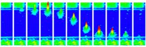
Fig 3-3: As researchers vary a voltage, the spot at
which electrons and holes collide and produce light moves along a
50-micron-long, 3-nanometer-wide carbon nanotube.
Nanotube coatings as heaters: A transparent lacquer containing CNTs can
be sprayed on any surface needing heating in any situation, like windscreens
& buildings. After it dries it would leave CNTs glued on the surface, on
applying voltage difference across it the CNTs would heat up acting as heaters.
Its main advantage would be that,
(1)
Even
if a part of the surface is damaged the remaining undamaged part will still
work.
(2) It produces uniform heating over the
surface.

Fig 3-4: The transparent lacquer
containing carbon nanotubes could quickly clear car windscreens of ice or
water. More powerful, opaque versions could even be used to heat homes
A square metre
of film about 0.3 millimetres thick provides around 15 kilowatts of heat –
enough to heat a good sized hall.

Fig 3-5: Thermal imaging shows
that the material can uniformly heat the surface it is sprayed onto(Image:
Domenik Nemec).
Ancient Damascus steel swords: Damascus
steel swords, first made in the eighth century A.D. in the

fig 3-6: A well preserved
Other applications are may be as below:
· A pair of nanotubes can be used as tweezers to move nanoscale structures on surfaces.
· Sheets of SWNTs can be used as electromechanical actuators, mimicking the actuator mechanism present in natural muscles.
· SWNTs may be used as miniaturised chemical sensors. On exposure to environments, which contain NO2, NH3 or O2, the electrical resistance changes.
4. Disadvantages & possible threats
A coin has two sides so, just like any other material CNTs have their own advantages & disadvantages.
4.1 Carbon nanotubes dangerous
when wet
Nanotubes are
hydrophobic, meaning they clump together in pure water rather than dispersing.
This led to the belief that they would not spread out when released by
factories into rivers and lakes. However, researchers at the Georgia Institute
of Technology in
4.2 Environmental hazards
“
This sheet of MWNT is believed to be very important for material science & its application, there will be endless uses of this sheet in the future.Perhaps this event is similar to the invention of plastic.
Years after the
invention, millions of applications, yet now (over)used so much that it causes
environmental problems. Nanotubes are very powerful but could be just as
dangerous as they are powerful in the human environment. One of the things that
is of prime concern is huge almost invisible ribbons or sails of this stuff
floating around in our oceans or in our atmosphere trapping and killing fish,
whales, birds, and 747's. Taking these fatal threats in account
4.3 Nanoparticles in air
Scientists are concerned with the problems of degraded nano particulate floating around and causing problems. Sure nano dust could cause people to have more asthma or worse. Carbon Arc spotlights and equipment produce soot, and carbon soot has been proven to increase the likeliness of cancer, both of a lung and skin variety. Any kind of fiber or tube or other structure that our bodies are not designed or adapted to cope with, when introduced into our biology, can and likely will cause complications unless dealt with or controlled.
Semi-degraded nanotubes would be having much the same effect as asbestos fibers in the lungs; injury, scarring, and ultimately formation of cancerous growths. Or have the same effect as fiberglass on the skin after long exposure: a dreadful irritant that can lead to long term rash and easy infection. A full, comprehensive and cautious health study needs to be conducted in the long term before we make these our latest "wonder material" to be overexploited without understanding.
5. Conclusion
After their discovery in 1952 by Russian scientists & coming under international focus in 1991 there has been immense research on CNTs around the world.
CNT’s role in future application & technology is truly promising. Their contribution to modern electronics, is surely to revolutionize the way we live, do our daily chorus & compute.
We must be very cautious with the use of these materials, because just as plastics that is now more a part of environmental problem due to overuse, materials made of CNTs which are predicted to be everlasting can also posses many such threats.