
Having built the kit, I felt there were a number of areas in which the kit instructions could be improved. I noted down all the areas where I had a few problems, and documented it all.
In addition, I think there are lots of possibilities to enhance the design. Things like an antenna tuner, an SWR meter, a power supply, additional bands, wider range VFO. The list goes on!
1. My set of instructions on how to build this kitset, including hints on some tricky areas
2. A corrected schematic
3. Some pictures of my build (Maybe there's something in these that will help the next person...), and
4. Some specifications on some of key components used in the KN-Q7 transceiver
Disclaimer: I have no association whatsoever with either FutureTech or BA6BF
Why did I create a new set of instructions? Doesn't the kit contain these?
Well, yes. The kitset does include some instructions. It's just there are quite a few little details that are not included. There were a few errors in a couple of places, and the schematic was a little difficult to follow... So, while the transceiver kit is quite straightforward to build for experienced builders, these instructions are intended to make the task easier for the rest of us. And besides, why repeat my mistakes?
These new instructions also follows my preferred method of construction -- One stage at a time.
Building the transceiver section by section, and testing each section as soon as you've completed it, allows any faults to be located more quickly. A fault is probably somewhere in that last set of parts you just added. Now, this is in stark contrast to the instructions provided with the kit. It suggest the opposite approach i.e. Build everything all in one go, and then test it. Well, fine. Personally, I find that is not the best approach. A fault can be very tough to find when you’ve got an entire board of parts and connections to check!
Anyway, I followed my step-by-step approach, and it worked. It also allowed me to break up the construction into a bunch of easy stages, with breaks well-timed for coffee.
But, hey, it's your kit, right? You choose!
1. Parts Inspection and Sorting
2. Surface Mount Devices - 3 chips to be soldered onto the PCB first
3. 8VDC regulator and rear panel sockets (Speaker and DC input)
4. Receiver audio
5. Second Mixer and BFO - Doubles as the transmit microphone amplifier and carrier oscillator
6. Transmit-Receive Power Supply Switching
7. Receiver IF Amplifier
8. IF Crystal Filter
9. First Mixer - Includes the Variable Crystal Oscillator (VCXO)
10. Receiver Bandpass Filter
11. Coil Winding
12. First Transmit Amplifier and Transmit Bandpass Filter
13. Second Transmit Amplifier
14. Third (Final) Transmit Amplifier and Low Pass Filter
15. Final Mechanical Assembly
(PDF file : 800k)
(PDF file : 66k)
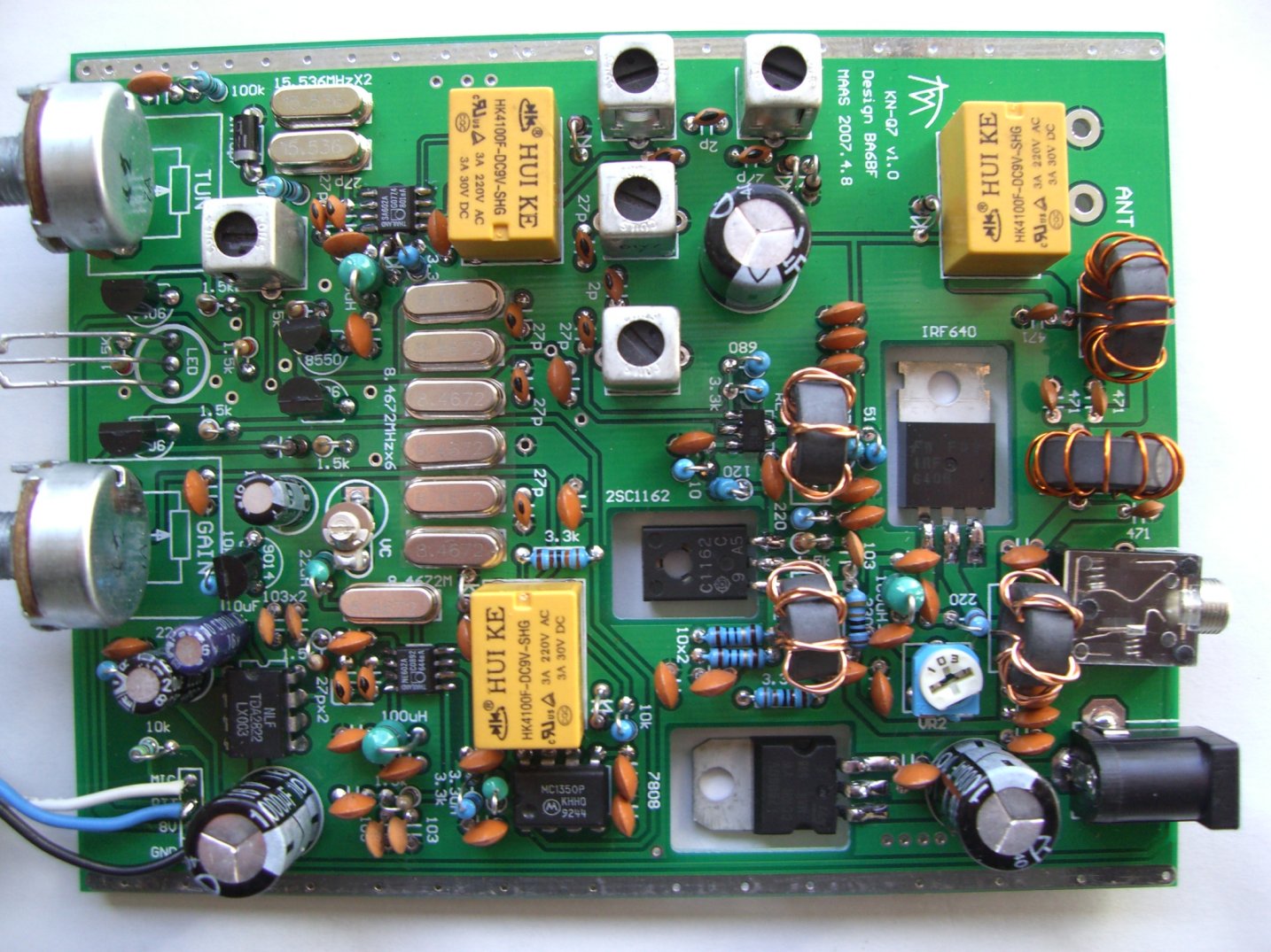
Stage 4 - Regulator and Receiver Audio completed
Stage 5 - Second Mixer and BFO built
Stage 7 - IF amplifier stage built
Stage 8 - IF cystal ladder filter
Stage 10 - First mixer, VCXO , and receiver bandpass filter
Stage 11 - Coils wound
Note: Full instructions, with more pictures, in the kit-build instructions )
Stage 12 - First Transmitter Amplifier and Transmit Bandpass Filter
Stage 13 - Second Transmitter Amplifier
Stage 14 - Third (Final) Transmitter Power Amplifier and Low Pass Filter
Stage 15 - Final Mechanical Assembly
Just click on the component for more details:
DIY7-7 coils
NE602 mixer/oscillator
MC1350 IF amplifier
TDA2822 audio amplifier
2SC3357 1st tx amplifier
2SC1162 2nd tx amplifier
IRF640B Final tx amplifier
Thanks to the various vendors and alldatasheets.com for many of these PDFs!

1. 1k5 and 10nF feedback components adjacent to 2SC1162 are missing (R25 and C50 on my schematic)
2. Relay coils and protection diodes are not shown (K1- K3 and D8 - D10)
3. 2SC3357 collector resistor is shown as 22 ohms rather than 27 ohms (R18)
4. Base bias resistor is shown as 56 ohms rather than 51 ohms (R22)
5. The optional fit 10k resistor used to provide 8V bias to the microphone is not shown (R7)
6. The 3k3 and 100nF bypass capacitor adjacent to the 10k FET bias preset are not shown (R30 and C55)
7. The 'SQL' label driving the audio mute transistor (Q1) via a 1k5 resistor (R11) is actually connected to +8VT
8. There is an additional +13.8VDC 100nF bypass capacitor adjacent to the 330 ohm resistor (C52)
Note: These corrections DO NOT apply to the schematic available from my site
An antenna tuner - so I can use a variety of antennas when I take this transceiver on my next holiday
A simple SWR meter - I shall probably build this into the antenna tuner
A 12V/2A power supply - I've already done some work on this, so details of this should be along soon
If I get a bit more time, and as I finish these off, I’ll put the details up on this site. Stay tuned!