Stereo Video Digitizer
The stereo video digitizer will
accept video input from 2 PAL CCD video camera. It digitizes the video
and display both the video sources on a PC monitor. My digitizer support
only greyscale video.
A software has been written
to display the digitized video on a PC monitor. There are 2 versions of
the sofware:
winepp standard
version, for still image capture
wineppx utilises
the Direct X 6.1 library. Requires Direct X 6.1 installed.
This is actually my university
thesis project. For simplicity, I convert the chapter 3 of my thesis into
this page, so all the pet label in this page start with 3.x. Please bear
with it. You can download my thesis
in MS Word format.( 1.1 MB)
The Hardware and Theory Description
In this chapter, the entire stereo video digitizer hardware is broken into
subtopics and explained. There is also a part on building the hardware
boardschematic design and PCB fabrication.
System Description

Figure 3.1 System Block Diagram
Basically, this project can
be separated into several main functional blocks. Each of these blocks
perform a specific task, which would be explained in the later section.
As a stereo video signal
(dual video sources) goes into stereo video digitiser, only one channel
is being chosen at one time by the Video Multiplexor. A video amplifier
will also amplify the video signal. The amplified video signal will
be route to an analogue to digital converter (ADC) to be converted into
digital raw data.
A Synchronization Separation
and video timing circuit is aimed to generate a suitable sampling clock
to drive the Analogue To Digital Converter (ADC), as well as the write
clock into the digital data storage.
Having digitise the analogue
video signal, it is stored in a digital data storage block. The data can
then be sent to a PC through the parallel port in Enhanced Parallel Port
(EPP) mode.
The control logic block
is meant for doing the handshaking signals required by the EPP protocol.
Video Input Multiplexing And Amplification
The CCD camera used in this
project is a PAL standard camera. Its output range from 0 to 1V.
As shown in figure 3.2,
the digitizer has 2 BNC header as input for 2 CCD cameras. The signal is
terminated using a 75W resistor, and fed into the MAX4313 video amplifier,
which will be explained in section 3.3.2.
Several ceramic capacitors
are used to decouple the voltage source to ground. This is for noise suppression
purpose on the power source, which will be explained in section 3.4.

Figure 3.2 Video Input, Multiplexing and Amplification
Both the video signals will
then be fed into a video-multiplexing amplifier, the MAX4313. Although
the stereo video digitizer has two video-input channels, only one channel
is routed to the Analogue to Digital Converter at one time. By using the
multiplexing feature of the MAX4313, only one video channel is selected
each time.
MAX4313 also provides a
fixed gain of +2V/V. This device has a 40ns channel switching time, low
10mVp-p switching transient, and a 150MHz 3dB bandwidth, making it ideal
for video switching application.
Synchronization Signal Separation
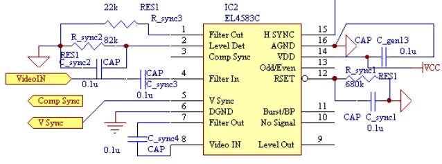
Figure 3.3 Sync Separation
The circuitry in figure 3.3
is used for extracting synchronization signal from the video input signal.
These sync signals are later used by other parts of the digitizer.
The Elantecs EL4583C is
used as sync separator. It is configured for extracting timing information
from a PAL video signal such as composite, vertical and horizontal synchronization,
burst/Back porch and Odd/Even field information.
The video signal, having
been amplified by the video amplifying circuitry, is fed into pin 4 of
the EL4583C. The IC has a built in 3 pole active filter to attenuate the
chroma signal to prevent colour burst from disturbing the sync slice.
Composite and Vertical Sync
outputs of the IC is used later throughout the stereo video digitizer circuitry.
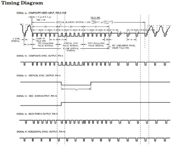
Figure 3.4 EL4583Cs timing information
Figure 3.4 shows the timing
diagram of the synchronization signal output of the EL4583C. Basically,
the IC isolates 5 different synchronization signals. They are composite
sync, vertical sync, odd-even output, back porch output, and true horizontal
sync.
The composite sync output reproduces
all the video input sync pulses, with a propagation delay.
Vertical sync leading edge is coincident with the first vertical serration
pulse leading edge, with a propagation delay.
Odd-even output is low for
even field, and high for odd field.
Back porch goes low for
a fixed pulse width on the trailing edge of video input sync pulses. Note
that for serration pulses during vertical, the back porch starts on the
rising edge of the serration pulse (with propagation delay).
Horizontal sync output produces
the true ``H'' pulses of nominal width of 5ms. It has the same delay as
the composite sync.
Video Timing ( Clock Generation )

Figure 3.5 Timing Circuit
Figure 3.5 shows the circuitry
where all the timing information needed by the digitizer hardware is extracted.
This includes the sampling clock used by the ADC and write clock used to
drive the SRAM (section 3.3.6).
The IC 74HC4017 counts past
the first 10 lines-some of which are in reality only half-length, and inhibits
collection of those-otherwise the captured picture would sometimes wrap-around.
Reset logic to 74HC74 is a crude attempt to give pseudo line locking of
what is essentially an asynchronous clock. The 74HC74 D flip flop in conjunction
with the 74HC4040 binary counter ensures a controlled number of samples
are made per video line (By setting the jumper at pin header H1). For example,
QA is 10 MHz, QB is 5 MHz and so on. For this project, a 20MHz oscillator
is used. 10 MHz is used as sampling clock to the ADC, while a ~5 MHz clock
for writing data to the digital storage block. This mean, we will get a
320 X 320 pixels video, with 8 bit per pixel.
T =1/f
=1/5M
Line Duration =320 * T
=64us
which is the same as the PAL line duration
Analogue To Digital Conversion

Figure 3.6 Analog To Digital Conversion
Figure 3.6 is the circuitry
for analog to digital conversion. Here, analog video input signal is sampled
at 10MHz, and an 8 bit digital data is obtained.
The TLC5540 8 bit
high speed ADC is used to convert the analogue video signal into digital
data. The ADC is always enabled, and running on a free running clock of
10MHz. It is configured for converting analogue signal in the range of
0.61V 2.63V. Ferrite Bead is used to give a clean undistorted supply
voltage as required by the ADC.
The data output lines of
the ADC is fed into the 74HC541 octal line driver for buffering purpose.
The enable pin of the 74HC541 is controlled in such a way that signal conflict
on the shared data line(Y1-Y8) will never occur.
Digital Data Storage

Figure 3.7 Digital Data Storage
Digital data storage is meant
for providing a temporary storage for the sampled digital video data prior
to transferring it to the PC. It is shown in figure 3.7. Basically, the
digital data storage block is made up of the TC551551CP-70L static random
access memory (SRAM), and some 74LS193 counter ICs. The TC551551CP-70L
acts as an asynchronous data buffer as the speed of data being written
into RAM is a lot faster than the speed of data being read from it.
The TC551551CP-70L is a
1M bit (or 128K byte) SRAM. It is chosen as the resolution of the video
been captured by the stereo video digitizer is at 320 X 320 pixels (8 bit/pixel).
This means a capacity of 100K byte is needed. The TC551551CP-70L
has a 70ns access time, which is sufficient for a 10 MHz sampling-clocked
system. (Note: 70ns is about 14.3 MHz). However, use of a faster SRAM is
recommended in improving the system performance. The only drawback is that
it is hard to find one in Malaysia.
The series of 74LS193 binary
counter connected in cascade is meant for generating address for the SRAM
address line. The output data pins of these counters are connected to the
address pins of the TC551551CP-70L. There is a Master Reset (denoted by
MR) control pin for resetting the address line to 0, and a Count Up (denoted
by CU) for counting up the address when there is a clock provided.
The WE control line on the
TC551551CP-70L is meant for controlling data read or write onto the SRAM.
When WE is low, the SRAM data pin is meant for input; when it is high,
the data pins are meant for output.
Control Logic And Enhanced Parallel Port Interfacing
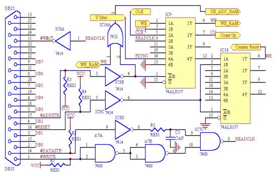

D0 through D7 (or pin 2 through 3 of IC 11) should be fitted with 4.7 kW
pull down resistor.
Figure 3.8 Control Logic and EPP interfacing
The circuitry in figure 3.8 is meant for generating handshaking signal
as defined by the IEEE1284 Enhanced Parallel Port protocol. Please refer
to figure 2.1 for timing diagram reference.

Figure 3 shows a typical
read cycle. During read cycle, write and data strobe will be held low by
the PC parallel port internal circuitry. On seeing this, IC8 and IC7 will
generate a high at the Wait control line, so that the PC will read data
from IC11 (74HC541 octal buffer). A pulse named READCLK is generated during
this process, which is used for clocking the CU pin of the digital storage
block.
Since the MR and CU of the
digital storage block should be controlled by the parallel port interface
logic during read cycle; but should be controlled by the analogue circuitry
of the video digitizer otherwise, a multiplexer is needed for selecting
the correct control signal at correct time for MR and CU. For this purpose,
two 74LS157 quad 2:1 MUX are chosen. The Address Strobe and Reset pin of
the EPP port are used as control line to drive these two MUX, since they
are not needed in the EPP handshaking.
During read cycle, the Address
Strobe is pull low to select READCLK for the digital storage CU. Reset
line should be pulse low for a short interval to reset the counter in the
digital storage block. In short, the counter will be reset, and data is
read out from the SRAM.
When the read cycle ends,
both Reset and Address Strobe are pull high. This will let the control
signals from the analogue circuitry (the sampling CLK and V Sync) to take
over the control over the CU and MR or the digital storage block. As long
as another data read cycle does not start, the SRAM is constantly been
updated with data sampled from the video signal.
Apart from that, the pulse
that is generated by the Reset line will also trigger the 74LS76 flip flop.
Configured as a toggle flip flop, the 74LS76 will let the stereo video
digitizer switch its video input channel whenever a complete frame of video
is transferred to the PC. With this approach, the PC can get a digital
stereo video source.
Power Supply

Figure 3.10 Power Supply
The stereo video digitizer needs +5V and 5V supply. The digitizer board
has circuitry onboard to provide a regulated +5V and 5V votage source,
as shown in figure 3.10. This part is also important in the sense
that it regulate the input voltage, and protect the digitizer board from
problem as over-current, spikes, and voltage surges.
The +5V supply is realized using a 7805 voltage regulator. ICL7660
is used for inverting the input power supply. A 7905 is used for generating
a regulated 5V supply. The main supply should be in the range of
79V.
Building the Hardware
Building the stereo video
digitizer involves 3 main steps. They are drawing the schematic diagram,
design and fabricate the printed circuit board and mounting the electronic
components.
For drawing the schematic
diagram, the Protel Advanced Schematic software is used (see figure 3.11).
A schematic diagram let us graphically connect different electronic together
in order to make up a circuit.

Figure 3.11 Protel Advanced Schematic schematic drawing software
After the complete schematic
of the stereo video digitizer is drawn, we will extract its netlist. This
netlist will be used in a subsequent software in the Protel family, the
Protel Advanced PCB, for designing the printed circuit board (PCB) layout.
Figure 3.12 shows a screen capture of the Protel Advanced PCB in action.
For this project, the circuit
board is designed in double-sided. This provides a more compact design.
When the design is completed,
we can fabricate it by sending it to any chartered PCB fabrication factory
for fabricating the PCB.
Lastly, when the PCB is
fabricated, we will mount the needed electronic components onto it.

Figure 3.12 Protel Advanced PCB
Due to time constraint, I only fabricate PCB for the analog part. The
digital part is done on strip board. You can download
the Protel PCB files which i've drawn here. However, their are scattered
not in sequence. Please refer to the circuit described in this page.
Known Problems and Limitation
The first limitation of
the stereo video digitizer is that it does not do any chroma signal filtering.
If a colour CCD camera is to be used, the colour burst chroma signal should
be attenuated prior to been sampled by the ADC. Otherwise, the video will
display unwanted herringbone pattern.
The CCD camera is connected
to the digitizer using a coaxial cable. Thus, the video input connector
should be terminated using 75W resistor to match the coaxial cable impedance.
The parallel port interface
is susceptible to noise. The control line Address Strobe and Reset from
the PC will cause unwanted result on the video grabbed if there are spikes
within the lines (which usually have). For example, a spike on the Reset
line might reset the address counter when it should not; whereas spike
in Address Strobe might incorrectly trigger the counter. A low pass filter
(simple RC network) should be connected to these lines to attenuate the
spikes. Actually, i didn't solve this problem in my project. It cause my
captured video to experience drift, a serious problem. Should somebody
fixed it, please email me.
Although the EPP interface
has a rated speed of up to 2 Mbyte / s, the actual data transfer cannot
achieve this speed. This is due to the fact that there are other hardware
delays within the digitizer circuitry, and software overheads at the PC
part.
In theory, to get a picture
with square pixel, a clock rate of 14.75 MHz for PAL should be used.
Since the stereo video digitizer
contains digital and analogue circuitry on the same board, current spikes
from the digital part may reach analogue part where they gets amplified
and cause errors, oscillations or instability within the whole analogue
circuitry. To solve this, the digital ground plane should be separated
from the analogue ground plane. The interconnection of the two separate
ground plane can e done on the most stable reference ground point of the
system (ie: the power supply ground point ).
Future Development
In order to improve the data transfer
rate of the digitizer, it can be ported to a faster bus (rather than EPP)protocol,
such as the ISA bus which has a clock of 4MHz. You can take a look on my
simple ISA prototyping board described elsewhere on my homepage.
The circuit design can be
greatly simplified by using a FIFO as digital data storage rather than
SRAM. This is due to the fact that a FIFO does not need any address line.
For example, there are FIFO from OKI, IDT and ISSI.
The digitizer can be used
for colour signal decoding through software. For a headstart, check out
W.A
Steer home-built video digitizer page.
Eventually, feel free to email me
on any issue relating to this project.