|
Atari XL PC
bridge
By Roland Scholz
After a short period of doing
nothing for our beloved Atari 8-bit, I am back with details of
the PC bridge interface project. This interface allows you to
connect several old-style ISA cards to your Atari. Up to now I
have successfully tried cards that provide Hercules graphics,
RS232 serial communication up to 38,400 baud and Centronics
printer interfaces in standard (unidirectional) mode. But this
is not the limit, I consider all the other cards: Adlib sound,
other graphics, Ethernet and so on.
|
|
|
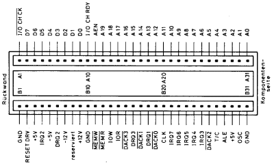
Figure 1: Pin
assignment of the PC(XT)
bus. |
In to order to keep the interface
compatible with the Atari and its operating system, I
developed the interface as a full-function PBI device. The
design of PBI devices has already been described in three
former MyAtari articles (issues 7, 9 and 10). In order to give
a first impression of the PC bridge design, I’ll introduce the
62-pin PC bus socket and tell you more about the function of
the pins used by the PC bridge. If you consider figure 1, you
will note the PC socket has signals for 8 data lines (D0-D7)
and 20 address lines (A0-A19). With 20 address lines you can
address a space of 2^20 = 1Mbyte memory cells. In a standard
PC this space is divided into two sections. The first one
forms a memory block of 640 Kbyte and the second 384 Kbyte are
reserved for memory (either RAM or ROM) located on adaptor
cards.
The next quite important signals
are the four control lines IOR\, IOW\, MEMR\ and MEMW\ that
control access to the I/O address space spanned by 16 address
lines and to the 1Mbyte memory address space. Unlike the 6502
processor, the Intel 80x86 architecture does not map
registers of I/O chips into the memory address space, but a
second I/O space is used. Thus, the MEMR\ and MEMW\ active-low
signals denote a read or write access to main memory,
respectively; whereas the IOR\ and IOW\ signals denote the
same for the I/O address space.
The next few lines to consider are
the interrupt lines IRQ2-IRQ7, that show a pending interrupt
request by pulling the specific line to a logical 1. The
interrupts are also prioritised such that IRQ2 has the highest
priority and IRQ7 the lowest. If a logical 1 is applied to the
line RESTDRV all plugged-in cards will be reset. The last
important signal is IOCHRDY, which shows whether the active
card needs another clock cycle to finish the active access.
This is called a wait-state and is used to connect slow cards
to faster processors. Indeed this a problem for us, since the
Atari manages a memory access in just one clock cycle, so one
acccess takes approximately 1/1.77 Mhz = 0.565 microseconds.
It is a fact that older PC cards are so slow, they only work
with frequencies at or below 1 Mhz or they use a wait-state to
refresh their on-board RAM (like Hercules cards do). For this
reason our PC bridge has to cope with these wait-states making
the design somewhat more complicated. One drawback is, for
instance, we have to use the processor signal SYNC that cannot
be obtained from the parallel bus, but has to be taken from
the CPU directly.
 Now please consider figure 2 below, a block
schematic of the PC bridge with its essential components. From
this figure we will go into detail if required. The interface
consists of several 8-bit latches, which store the address
information on the PC side, an 8-bit bi-directional tri-state
register and line buffer, a single 8KB EPROM and a 8KB static
RAM (of which we will only use 1KB). The other elements act as
decoders to form select and data-strobe signals. GAL (Generic
Array Logic) chips are used to quickly form the desired
operations. The main design implements a PBI device that maps
its driver ROM into the 2KB area that is usually occupied by
the Math-ROM from $D800 to $DFFF. This area is then divided
into four sections. The section from $D800 - $DBFF (1KB)
belongs to the driver EPROM that contains the driver firmware.
Obviously 1KB would be too small for all the drivers, so we
can map eight 1KB pages of the EPROM into this area (the EPROM
has 8KB arranged into eight 1KB pages and only one of these
can be accessed at a time). We have four spare bits on one
register from which we use three bits to map to pages using
the EPROM’s address lines (A10-A12). When programming drivers
we have to keep track of the pages we are in. This certainly
diminishes the performance of the PC bridge a little bit, but
this is better than expanding the design any further. The
fourth free bit we connect to the address line A9 of the RAM
giving us two pages of 512 bytes at the location from $DC00 -
$DDFF. Table 1 again lists the used areas. Now you might ask
how we are able to address the 1MB memory space and the
64KB I/O space with only two 256-byte pages. This is
simple, we just write the missing 12 or 8 most signifiant
address bits to the registers. Again, we lose some
performance, but most of the time we do not have to reset
those bits. All in all we get a quite acceptable performace
without having to build overly complex hardware. Now please consider figure 2 below, a block
schematic of the PC bridge with its essential components. From
this figure we will go into detail if required. The interface
consists of several 8-bit latches, which store the address
information on the PC side, an 8-bit bi-directional tri-state
register and line buffer, a single 8KB EPROM and a 8KB static
RAM (of which we will only use 1KB). The other elements act as
decoders to form select and data-strobe signals. GAL (Generic
Array Logic) chips are used to quickly form the desired
operations. The main design implements a PBI device that maps
its driver ROM into the 2KB area that is usually occupied by
the Math-ROM from $D800 to $DFFF. This area is then divided
into four sections. The section from $D800 - $DBFF (1KB)
belongs to the driver EPROM that contains the driver firmware.
Obviously 1KB would be too small for all the drivers, so we
can map eight 1KB pages of the EPROM into this area (the EPROM
has 8KB arranged into eight 1KB pages and only one of these
can be accessed at a time). We have four spare bits on one
register from which we use three bits to map to pages using
the EPROM’s address lines (A10-A12). When programming drivers
we have to keep track of the pages we are in. This certainly
diminishes the performance of the PC bridge a little bit, but
this is better than expanding the design any further. The
fourth free bit we connect to the address line A9 of the RAM
giving us two pages of 512 bytes at the location from $DC00 -
$DDFF. Table 1 again lists the used areas. Now you might ask
how we are able to address the 1MB memory space and the
64KB I/O space with only two 256-byte pages. This is
simple, we just write the missing 12 or 8 most signifiant
address bits to the registers. Again, we lose some
performance, but most of the time we do not have to reset
those bits. All in all we get a quite acceptable performace
without having to build overly complex hardware.
At this point we go into detail and
take a closer look at the interrupt circuit. We certainly need
interrupts, since without them, we would not be able to build,
for example, a reasonable RS232 interface. Especially here it
is important to quickly get the data out of the chip and
written to a buffer. If this is not done in time the data get
overwritten by the next incoming data and we and up with
corrupted data. Since the Atari only has two interrupt lines
(NMI and IRQ) of which just IRQ is connected to the parallel
bus, we have to wire the six IRQ signals from the PC bus using
diodes to a 74LS74 flip-flop. It stores the interrupt
information during the leading edge of a IRQ2-7 signal (figure
3, top-left). The inverting output is used to connect the
signal to Atari’s IRQ\ line. An LED also shows the state of
the interrupt latch. The latch is reset by a reading access to
ISAMEM or ISAIO. To accomplish this, the signals IOR\ and
MEMR\ are combined using two diodes and a resistor. I figured
out that sometimes the output level is not suitable to drive
the latch’s CLR\ input low, so I amplified the signal by two
free inverters. This is not (yet) shown in the schematic
and may not be necessary if only 74HCTxxx TTL chips are used
(I took a 74LS74 for convenience). In order to conform to the
PBI specification we must ensure that the PBI device causing
the interrupt drives low its corresponding bit in the NEWPORT
register. To do this, we connect the latch’s output Q to GAL2,
which takes care of this.
|
Address |
Assignment |
|
$D800 - $DBFF |
ROM 8 x 1 KB |
|
$DC00 - $DDFF |
RAM 2 x 512
Bytes |
|
$DE00 - $DEFF |
I/O address space
PC |
|
$DF00 - $DFFF |
Memory address space
PC |
|
PBI register |
Assignment |
|
NEWPORT $D1FF |
Turn on/off PBI device, IRQ
triggered? |
|
ISAHI $D1FE, IC3 –
74HCT573 |
Bit 0-3: address signals PC
bus A16-A19
Bit 4-6: PBI ROM Page0 –
Page7
Bit 7: PBI RAM Page0 /
Page1 |
|
ISALO $D1FD, IC2 –
74HCT573 |
Bit 0-7: address signals PC
bus A8-A15 |
|
ISADATA $D1FC, IC4 –
74HCT651 |
Bit 0-7: PC data bus read
D0-D7 |
|
|
|
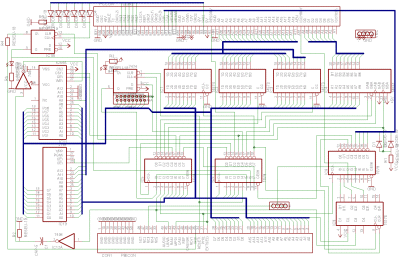
Figure 3: Schematic of the
PC bridge interface. At the top-left are the diodes and
the latch that stores incoming interrupt information.
Below are the RAM and ROM that contain driver software
and local variables. The 2 x 8 jack in the middle is the
latch to switch the PC bridge on and off. To the right
are the latches that store address and data bus
information.
[Click to
enlarge] |
The last thing I want to explain in
detail is the management of wait-states, which has taken most
of the development time (not mentioning the programming of
driver software which is still not finished) and technically
interesting. Due to the reasons mentioned above we cannot
access the PC bridge synchronously. We have to implement some
intelligence enabling the interface to handle read or write
accesses independently from the Atari. First we take a look at
the easier write access. If the Atari wants to write to a PC
card, all required information is put to the address and data
bus and the R/W\ signal drives low level. If this is the case,
the PC bridge stores the lower eight address bits in the
leftmost latch and the data bus is stored in the 8-bit
bidirectional register (74HCT651). Next the MEMW\ or IOW\
signal is driven low for one clock cycle, unless the card
signals a wait-state condition using the IOCHRDY line. If the
wait-state is signalled, the write signal is held low for as
many clock cycles as the the IOCHRDY is active. Since, as a
rule of thumb, the PC card accepted the data in 1 up to 3
cycles, the time to get the data into the card does not
conflict with following accesses.
Now we consider a read access to a
PC card. Here again the lower eight address bits are stored in
the leftmost register. This time the R/W\ signal drives high
level which causes IOR\ or MEMR\ to go low. This again is done
for one clock cycle, unless the PC card signals with the
IOCHRDY line that it needs the signal somewhat longer. If
eventually the read access has been finished, the data read
are stored in the bidirectional latch 74HCT651. A read command
like LDA $DE00 does not yield to valid data transferred into
the accumulator, but the data are only stored in the latch.
For this reason I implemented a read access to the latch at
address $D1FC that still belongs to the PBI config register
space. Thus, a full reading access to a PC card looks like
this:
LDA
$DE00
(ISAIO)
LDA
$D1FC
(ISADATA)
Now we come to talk about the
somewhat disturbing fact that it's neccessary to use the SYNC
signal that is not connected to the parallel bus. Assume we
issue a LDA $DE00,X command: This statement takes 4-5 clock
cycles, one for loading the opcode, two to load the address
($00, $DE), one to add the X-register to get the effective
address and one cycle (only if a page-boundary is crossed) to
read data at the effective address. It is a feature (or a
bug?) of the 6502 processor to put the absolute address
(without the X-register added) on the address bus during the
third cycle. The PC bridge now thinks it has been addressed
and the above described process takes place. At the next cycle
the processor has added the X-register and again put the
address on the address bus. But since the PC bridge has been
triggered before, it cannot cope with this request and will
yield incorrect data. Unfortunately, programming
storage-intensive applications cannot reasonably be done
without indexing capabilities, so we have to find a way out of
the maze. The way we look is to use the SYNC signal which
tells us wether the active cycle is an opcode fetch. So the
interface has a way to determne if the last statement has come
to an end and can start processing the request. If you have
any idea how this could be done in a better or simpler way,
please give me a hint, for I really do not want to use signals
that are not connected to the parallel bus.
The rest of the circuit is just
some stuff you will get to know if you analyse the schematic a
little it closer. I recommend reading the GAL programms
thoroughly and please take care of GAL3 that handles the
wait-states and SYNC signal unsing a state-machine. The last
figure shows the complete schematic.
I would be glad if this article has
been interesting to you, and want to encourage you to take
part in this project to push it forward. If you want to peek
into the stuff, please take a look at my web page for this
project where you can find all articles, schematics and so
on.
At this time there are drivers for
Hercules graphic cards, up to four RS232 serial interfaces and
up to three parallel interfaces. Only a configuration tool has
to be finished to get a working device and there are still a
lot of cards left that want to be used with an Atari
computer.
|
|
Appendix
Programs for GAL1, GAL2 and GAL3
(all type 16V8).
|
GAL16V8
Gal1 PcBridge
V2.0
D BUSIO RW PHI2 A11 A10
A9 A8 A1 GND
A0 R0W R1W R2W R3R ROM
RAM ISA R0R VCC
/R0W = D * /A11 * /A10 * /A9
* A8 *
A1
*
A0 *
PHI2 * /RW
R0R = D * /A11 * /A10 * /A9
* A8 *
A1
*
A0 *
PHI2 *
RW
R1W = D * /A11 * /A10 * /A9
* A8 *
A1 *
/A0 * PHI2 * /RW * BUSIO
R2W = D * /A11 * /A10 * /A9
* A8 * /A1 * A0 * PHI2 * /RW *
BUSIO
/R3R = D * /A11 * /A10 * /A9
* A8 * /A1 * /A0 * PHI2 * RW *
BUSIO
/ROM = D * A11 * /A10 * PHI2
* BUSIO
/RAM = D * A11 * A10 * /A9 *
PHI2 * BUSIO
/ISA = D * A11 * A10
*
A9 *
PHI2 * BUSIO
DESCRIPTION
/R0W : CLK signal for the
NEWPORT latch at $D1xF (write
access)
R1W : CLK signal for the
ISAHI latch at $D1xE
R2W : CLK-Signal for the
ISALO latch at $D1xD
/R3R : Strobe signal to read
from ISADATA at $D1xC
/ROM : OE signal for the ROM
at $D800-$DBFF
/RAM : OE signal for the RAM
at $DC00-$DDFF
/ISA : Signal that indicates
access at $DE00-$DFFF
R0R : Signal to read from
NEWPORT latch at
$D1xF | |
|
Module
gal2;
gal2 Device
'p16v8';
Declarations
"
Inputs
A15, A14, A13, A12, A11,
RESET, BUSIO, PCIRQ Pin 1, 2, 3, 4, 5, 6, 7,
8;
R0R, WRITE,
ISA
Pin
9, 11, 15;
"
Outputs
MPD, D, RESETDRV, D0_7,
WRITE1, ISA_INV
Pin
12, 13, 14, 16, 17, 19;
Equations
!MPD
=
A15 & A14 & !A13 & A12 & A11 &
BUSIO;
D
=
A15 & A14 & !A13 &
A12;
RESETDRV =
!RESET;
ISA_INV = !ISA;
WRITE1 = WRITE;
D0_7
=
PCIRQ;
D0_7.OE = R0R;
End | |
|
Module
gal3
gal3 Device
'p16v8';
Declarations
q0,
q1
Pin
12, 13 Istype 'reg';
clr, write, ior, iow,
memr, memw
Pin
14, 15, 16, 17, 18, 19;
isa, a8, rdy, rw,
sync
Pin
2, 3, 4, 5, 6;
State_Diagram [q0,
q1]
state
0:
clr = 1;
write =
0;
memr = 1;
memw = 1;
ior = 1;
iow = 1;
if (isa & sync) then
1
else
0;
state
1:
clr = 1;
write =
!rw;
!memr = rw &
a8;
!memw = !rw &
a8;
!ior = rw &
!a8;
!iow = !rw &
!a8;
if (!rdy) then
1
else
2;
state
2:
write =
0;
clr
= 0;
memr =
1;
memw
= 1;
ior = 1;
iow = 1;
goto 0;
state
3:
goto 0;
End | | |
![[ Advert ]](PCBridge_eng/banner.gif)

