by Roland Scholz
 This series
of articles is dedicated to the so-called Parallel Bus
Interface (PBI). The first part considers the several
hardware signals of the PBI, the second one describes
the hardware needed to form a PBI-device and the third
article shows how this device is connected to the operating
system by software. This series
of articles is dedicated to the so-called Parallel Bus
Interface (PBI). The first part considers the several
hardware signals of the PBI, the second one describes
the hardware needed to form a PBI-device and the third
article shows how this device is connected to the operating
system by software.
As you know, our beloved Atari was
developed and built by talented engineers, who had the
foresight to give it the ability to connect up to eight
devices on a parallel bus.
Yet where can that parallel bus be
found and what sort of devices use it? If you take a
look at the back of the Atari 600XL or 800XL, you will
see an ominous lid labelled, "PARALLEL BUS".
If the lid is removed 50 silver pins, 25 on each side,
will smile at you. And they emit something else: performance!
As the term "parallel bus" suggests, the data
are not tranferred serial, bit by bit, but parallel,
which means 8 bits at a time. This is not even done
at the pace of 19,200 baud, as the serial bus does,
but at the maximum pace of the 6502 CPU. However, this
printed circuit board connector is directly linked to
most important signals of the CPU and contains signals
to embed a device in a plug & play manner. So now
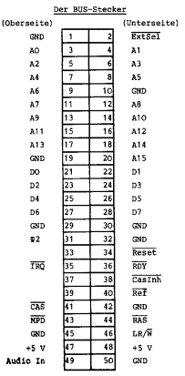
it is time to take a closer look at the pins as they
are shown in figure 1 (see left):
In the following description the backslash
(\) denotes a signal, which is active when the wire
has a voltage of 0V or, in the diagram, a bar is used
to show this.
The data-flow directions "in"
and "out" are seen from the CPU or from the
bus, respectively.
A0-A15, out:
These are the address
signals of the processor. Every time data are transferred
over the data bus, the CPU signals with these wires
which storage location is meant to transmit or receive
data. Since there are 16 address signals and each signal
can assume two states (0V or +5V), the Atari is able
to address 2^16 = 65,536 locations of storage.
D0-D7, in-out:
The effective data
are transferred using these lines. Since there are 8
of these lines, our Atari belongs to the so-called 8-bit
computers.
Reset\, out:
When the Atari is
switched on or the reset button is pressed, this line
goes low (0V) for a short time. Because of that, many
of the internal chips are initialized and the processor
starts to execute machine code that begins at the address
stored in the location $FFFC-$FFFD. Usually the operating
system (OS) ROM covers this area.
PHI2, out:
This line provides
for the system clock of the computer. It controls how
long a memory access takes and when it is finished.
PHI2 oscillates with a frequency of roughly 1.77 MHz,
so one oscillation takes only 1/1,770,000 = 0.565 microseconds.
In the first half of the oscillation PHI2 drives low
level, it switches to high level during the second half.
That means all memory accesses have to be finished by
the falling edge of PHI2.
LR/w, out:
This signal is called
"latched read/write". It is generated by the
CPU to show if the actual memory access is a read or
a write access and it is latched internally by the Atari
hardware. If the LR/w drives high level the CPU is to
read data from memory, in the other case the data are
to be written from to CPU to memory.
IRQ\, in (interrupt request, open
collector)
This signal tells the CPU it is to be
interrupted. Due to this line, the CPU or the program,
respectively, does not have to poll a certain line,
but the currently running program will be stopped, the
CPU registers are saved and the CPU starts to execute
the program whose starting address is stored at $FFFE-$FFFF.
As you might expect, these locations are covered by
the OS as well, so that the OS first takes control in
order to see whether there are keys pressed or data
are to be transferred over the serial bus (floppy, printer...).
When that is done, the CPU resumes execution of the
interrupted program.
RDY\, in:
This line gives an opportunity
to stop the CPU for a short time. Since the custom chip
ANTIC heavily uses this line as well, it is difficult
to use this line without disturbing both chips.
MPD\, in:
This signal is called
"math pack disable" and is used by an external
hardware to switch off the floating point routines located
in a ROM that reaches from $D800-$DFFF (2KB). If this
is done, you are free to put another ROM containing
drivers or peripheral hardware there. However, when
your own ROM is switched in, you cannot use the floating
point routines, if you do not want your system to crash.
EXTSEL\, in:
If this line is held
low during a memory access, the internal RAM of the
Atari is not accessed. This signal is usually used in
conjunction with MPD\, so the math-ROM and the internal
RAM are deselected and a user ROM may be accessed for
that cycle. Another usage is the 64KB expansion for
the Atari 600XL, which turns off the internal RAM using
this line.
CasInh\, out:
This signal drives
low level, if the Atari performs a RAM access. Otherwise,
if ROM or I/O chips are selected, this signal will go
to high level.
REF\, out:
The ANTIC chip is responsible
for refreshing the dynamic RAM every few milliseconds.
If the actual memory is a so-called refresh cycle, this
signal will show low level.
RAS\, CAS\, out:
The internal
structure of dynamic RAM is formed like a matrix. Each
storage cell is addressed by row and a column. So the
Atari has to split its 16-bit address into two addreses
for the internal matrix and generate these two strobe
signals (row addres strobe, column address strobe),
so the RAM knows when each address is valid.
AUDIO IN, in:
With this line,
you can mix your own audio signal to the sound generated
by the POKEY chip.
Now all the signals of the parallel
bus interface have been described briefly. The next
part of this series will show how these signals can
be used to form a device that is noticed and initialized
by the Atari during the power-up procedure. If there
are questions or suggestions, please write a couple
of lines to roland_scholz@web.de |
![[ MyAtari Advert ]](images/banner.gif)
