Warning: If you are here then you agree that I cannot be held at fault
should you damage your hardware as this is untested/unprove content.
Please note that if you have tired to contact me in the
past using the address below and got no reply chances
are you were filtered out as spam. So please post your
question to the eMachine Upgraders forum.
Tools Needed:
1x Soldering Iron
1x New very small/fine tiped solder tip
1x Some solder lead
4x 10K Resistors
Some Small wires.
Some free time.
Before doing this you should remove the motherboard from the case and
remove everything from the motherboard (such as cpu and ram and such)
just to be safe and for extra free space. Make sure youre discharged
of any static electricity and wear an anti-static wrist strap.
It should be noted I havent tested this and its only theory as I havent
a motherboard with the ICS 9248-99 Clock Generator. If you test this
and find it to work please please email me at:
-e-n-i-g-m-a--d-e-a-d-s-o-u-l-s- -a-t- -y-a-h-o-o- -d-o-t- -c-o-m-
(remove all dashes, replace "-a-t-" with "@" and "-d-o-t-" with "."
I do that so the spam bots do not pick up my email address)
Its recomended you do some cpu benchmarks before and after to see what kind
of performance gain you might have gained! You might use SiSoft's Sandra or
some other popular benchmarking test to get a good idea. When emailing me
send me your test results and screenshots as long as they are under 640x480
and 50kb in size.. also send me pictures of your moded ICS 9248-99 PLL,
and give me your website info if you wish for me to post it at the bottom of
this page.
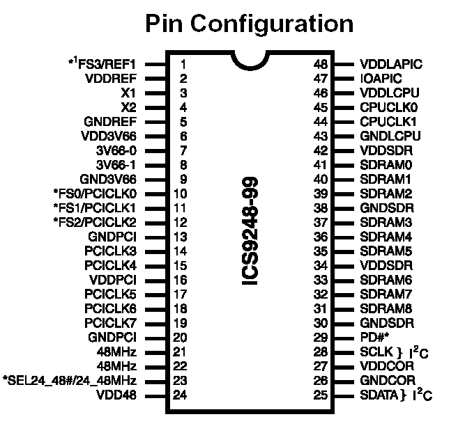
Here is an image of the Pin-Out of the ICS9248-99.
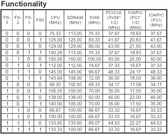
Here is an list of supported FSB's of the the ICS9248-99
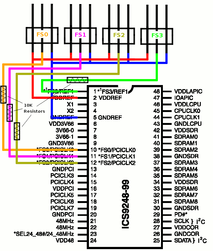
We are going to leave all of the pins connected as they are all I/O pins.
First we need to connect power to the jumper blocks for logic "1", to do
this we will use VDDREF (Pin 2) which supplies a nice 3.3v. Connect VDDREF
to pin 1 on the jumper blocks like shown in the picture below. Now we need
to connect ground to the jumper blocks for logic "0", however according
to the ICS9248-99 datasheet all the FSx Pins are connected internally to
ground so leaving them open should also in theory set logic "0". However
for this demonstration we are going to connect GNDREF (Pin 5) to pin 3
on all of the jumper blocks like shown in the picture below. Need we are
going to connect FS0 (Pin 10) to pin 2 on the first jumper block with a
10K resistor inline, then FS1 (Pin 11) to pin 2 on the second jumper
block with a 10K resistor inline, then FS2 (Pin 12) to pin 2 on the third
jumper block with a 10K resistor inline, and finally FS3 (Pin 1) to pin 2
on the fourth jumper block with a 10K resistor inline, all like shown in
the picture below.
Now to overclock, using the FSB chart above, if it calls for a logic "1"
on FS0 connect the FS0 jumper block middle FS0 pin to the VDDREF
pin on the jumper block, if it calls for logic "0" connect the middle
FS0 pin to the GNDREF pin on the jumper block. The same hold true
for all of the pins. Using the above FSB chart as a key it will tell
you what to set each pin to for various FSB's.
Wrote up at:13:32 PM EST, Saturday, March 13th, 2004 - Revision 0
Wrote by: Enigma Deadsouls
Website: http://www.oocities.org/enigmadeadsouls
Names/Info from people who have emailed me their test results:
None at this time.
You are free to mirror this page as long as you give me credit and do not change
any of the info unless you ask me first... however youre free to change text
font,size,color background color/image to match youre site. Youre also free to
remove my navigation bar at the bottom of this page as Im sure it would be
pointless on your site... in other words Im ok with changes as long as its not
to the info unless otherwise aproved by me. Also if you mirror it email me and
give me a link and Ill link to it here.