
Band Theory of Solids
As you might have already read, or remember from chapter 13, crystalline solids consist of atoms bound together in regular arrangements.
An atom consists of a heavy,positively-charged nucleus, surrounded by a cloud of light, negatively-charged electrons.
Energy changes must also be in specific amounts-energy is said to be quantized. The alllowed atomic energy are called energy levels. Each electron in a solid must have its own energy level.
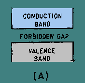
These individual levels are very close together in a band. Bands are seperated by values of energy that electrons are not allowed to have.
These energies are called forbidden gaps. Electrical conduction in solids explain in terms of these bands is called band theory.
Conductors
In conductors, the lowest band is only partially filled. Also in a conductor, the higher energy level is only a little above the normal level. Because of this, electrons can gain energy from the field and move from one atom to the next, this is called "conduct electricity." Electrons in a conductor have very high random speeds like atoms in a gas. Also conductivity is the reciprocal of resistivity. As conducitivity is reduced, the material's reistance rises.
EQUATION: free e-/(cm)3 Cu
Insulators and Semiconductors
In insulators, all levels in the lowest band, the valence band, are filled. It is called the valence band because, the electrons are the valence electrons of the atoms. An electrictic field cannot normally give an electron enough energy to reach the conduction band in insulators.
Conduction band is the energy levels electron would have to be in if they were to move in a band. Semiconductors are usually made of atoms with four valence electrons.
Atoms of the most semiconductors are silicon (Si) and germanium (Ge). The four valence elctrons are involved in binding the atoms together into the solid crystal.
After this is done, they are held togetherto form an individual atom. These valence electrons form a filled band, but unlike in an insulator, the forbidden gap is much smaller between the valence and conduction bands.
An atom from which an electron has broken free is missing an electron and is said to contain a hole.
A hole is an empty enrgy level in the valence band. Energy of electrons is in the conduction band while the holes have enrgies in the valence band.
Pure semiconductors that conduct as a result of thermally freed electrons and holes are called intrinsic semiconductors. Since so few electrons or holes are available to carry charge, conduction in intrinsic semiconductors is very small; their resistance is very large.
EQUATION: a. Si atoms/(cm)3 b. free e-/atom Si
Doped Semiconductors
To make a practical device, the conductivity of semiconductors must be increased greatly. This can be done by adding certain other atoms, or impurities, creating extrinsic semiconductors. Impurity atoms, often called dopants, increase conductivity by adding either electrons or holes.
The energy of this donor electron is so close to the conduction band that thermal energy can easily remove it from the impurity atom, putting an electron in the conduction band.
A semiconductor that conducts by means of electrons is called an n-type semiconductor because conduction is by means of negatively-charged particles.
Atoms in group three of the periodic table make extra holes, resultng in p-type semiconductors.
Only a few dopant atoms can produce large increases in conductivity.
Thermometers use the variation of conductivity of semiconductors with temperature.
Light detectors use the increase of conductivity of semiconductors exposed to light.

29.2: Electronic Devices
Diodes
A diode is made of one n-type and one p-type semiconductors that are next to each other. Rather than joining two seperate pieces of doped silicon, a sinlge sample of intrinsic silicon is treated with a p-dopant, then with a n-dopant.
The boundary between the p-type and n-type regions is called te junction. The resulting device is called an pn-junction diode.
The region around the junction is left with neither holes nor free electrons. This area, depleted of charge carriers, is called the depletion layer.
A diode with its n-type end connected to the positive battery terminal is reverse-biased. Almost no current flows. The diode is a reversed-biased diode.
With futher increases in voltage from the battery, the current increases. The diode is a forward-biased diode.
Diodes can convert AC voltage to voltage with only one polarity.
Diodes can do more than provide one-way paths for current. Diodes made from combinations of gallium and aluminum with arsenic and phosphorus emit light when they are forward-biased.
Diode lasers are used in CD players and supermarket bar-code scanners. They are compact, powerful light sources.

Transistors and Integrated Circuits
A junction transistor consists of a region of one type of doped semi-conductor sandwiched between layers of the opposite type.
A transistor consists of three alternating n- and p-type layers called the collector, base, and emitter.
A small current through the base-emitter junction causes a large current from the collector to the emitter.
Transistors are used as amplifiers in almost every electronic instrument. In a tape player, they are amplified to move the speaker coil. In computers, they can turn on or off large currents in the collector-emitter circuits.
Several transistors can be connected together to perform logic operations or to add numbers together. In a situation like this they are acting as fast switches, not amplifiers.
An integrated circuit, or microchip, consists of thousands of transistors, diodes, resistors, and conductors each no more than a few micrometers across.
An integrated circuit is constructed on a slice of a single crystal of silicon.
A single exposure to dopants produces resistors. Two exposures result in diodes, three in transistors.
Description of Solid State Electronics ·
Menu ·