All data sheets, the GAL assemblers easyABEL (DOS) and ISP Synario (Windows), PALtoGAL.EXE and the document GALCROSS.PDF are freely available for download at http://www.latticesemi.com, but no information on how to program the chips (see http://www.repairfaq.org/filipg/HTML/LINK/F_pal_gal.html).
If you would like to or have to write the software yourself:
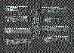
Pin assignment of the different GAL chips during programming
|
|
GAL |
16V8 |
18V10 |
20V8 |
22V10 |
6001 |
26CV12 |
|
|
1(2) |
VIL |
VIL |
VIL |
VIL |
VIL |
VIL |
|
|
2(3) |
EDIT |
EDIT |
EDIT |
EDIT |
EDIT |
EDIT |
|
|
3(4) |
RA1 |
RA3 |
RA1 |
P/V- |
VIL |
P/V- |
|
|
4(5) |
RA2 |
RA4 |
RA2 |
RA0 |
RA0 |
RA0 |
|
|
5(6) |
RA3 |
RA5 |
RA3 |
RA1 |
RA1 |
RA1 |
|
|
6(7) |
RA4 |
SCLK |
VIL |
RA2 |
RA2 |
RA2 |
|
|
7(9) |
RA5 |
SDIN |
VIL |
RA3 |
RA3 |
VCC |
|
|
8(10) |
SCLK |
STB- |
RA4 |
RA4 |
RA4 |
VIL |
|
|
9(11) |
SDIN |
SDOUT |
RA5 |
RA5 |
RA5 |
RA3 |
|
|
10(12) |
GND |
GND |
SCLK |
SCLK |
SCLK |
RA4 |
|
|
11(13) |
STB- |
VIL |
SDIN |
SDIN |
SDIN |
RA5 |
|
|
12(14) |
SDOUT |
VIL |
GND |
GND |
GND |
SCLK |
|
|
13(16) |
VIL |
VIL |
STB- |
STB- |
STB- |
SDIN |
|
|
14(17) |
VIL |
VIL |
VIL |
SDOUT |
SDOUT |
STB- |
|
|
15(18) |
VIL |
VIL |
SDOUT |
VIL |
VIL |
SDOUT |
|
|
16(19) |
VIL |
RA2 |
VIL |
VIL |
VIL |
VIL |
|
|
17(20) |
VIL |
RA1 |
VIL |
VIL |
VIL |
VIL |
|
|
18(21) |
RA0 |
RA0 |
VIL |
VIL |
VIL |
VIL |
|
|
19(23) |
P/V- |
P/V- |
VIL |
VIL |
VIL |
VIL |
|
|
20(24) |
VCC |
VCC |
VIL |
VIL |
VIL |
VIL |
|
|
21(25) |
|
|
RA0 |
VIL |
VIL |
GND |
|
|
22(26) |
|
|
P/V- |
VIL |
VIL |
VIL |
|
|
23(27) |
|
|
VIL |
VIL |
P/V- |
VIL |
|
|
24(28) |
|
|
VCC |
VCC |
VCC |
VIL |
|
|
25 |
|
|
|
|
|
VIL |
|
|
26 |
|
|
|
|
|
VIL |
|
|
27 |
|
|
|
|
|
VIL |
|
|
28 |
|
|
|
|
|
VIL |
PLCC28 pin numbers of DIL24 chips in paranthesis
Inserting the chip
You should turn off the socket to allow for insertion of the chip, by asserting a voltage difference below 0.7 volt between any of the pins. The pins should not remain open, as an open wire may have any (static) voltage, but should be connected using (4k7) resistors to the same potential. This is accomplished by pull-ups or pull-downs and turning off VCC to which the pull-ups are connected.
Power-up
Before a GAL can be programmed you have to apply the supply voltage and the programming voltage to the chip. You have to connect VCC first. The GAL will show its programmed behaviour, that means that some output pins work as outputs and some as inputs. You have to assert valid logic levels on the inputs, and because you can not tell which outputs are actually working as inputs, you have to apply these levels using pull-up or pull-down resistors. Therefore you have to use 4k7 pull-down on all VIL pins and 4k7 pull-ups on all other pins. After the chip has powered up you may apply 12 volt to EDIT to switch the chip into the programming mode. The pins will switch to the function they have in the programming mode, so again some inputs may become outputs, other outputs may turn off. The pull-ups will handle this nicely, and assert a state that will not allow the chip to modify itself. Now you may turn on the drivers.
Initialize
Set all pins (except GND, VCC, EDIT and SDOUT of course) of the GAL to L, except STB- which should stay H.
Read (16V8/20V8) at 12 volt on EDIT:
Set P/V- to L, set up the desired pattern on RA0..RA5, bring STB- for a short time (1-10us) to L and again up to H, read bit from SDOUT, bring SCLK to H for a short time (1-10us) and back to L and read the next bit until all bits of this line are read.
Write, Erase, Security fuse (16V8/20V8) at VPP volt on EDIT
Set P/V- to H, set up the desired pattern on RA0..RA5, apply first bit to SDIN, bring SCLK for a short time to H and back to L, and transfer the next bit until all bits of this line have been transferred. Bring STB- to L and wait for the programming pulse time before you take it back to H again. Restore P/V- to L at the end of the operation.
Read (other) at 12 volt on EDIT
Set P/V- to L, set up the desired pattern on RA0..RA5, set bit (a L for fuses, else H or L as required for address) to SDIN, take SCLK for a short time (1-10uS) to H and back to L and transfer the next bit until all bits of the line are transferred. Bring STB- for a short time to L and again up to H, read bit from SDOUT, bring SCLK to H and back to L and read the next bit until all bits of this line are read.
Write, Erase, Security fuse (other) at VPP volt on EDIT
Set P/V- to H, set up the desired pattern on RA0..RA5, set bit to SDIN, bring SCLK for a short time to H and back to L, and transfer the next bit until all bits of this line have been transferred. Set SDIN to L and bring STB- to L and wait for the programming pulse time before you take it back to H again. Restore P/V- to L at the end of the operation.
Power-Down
You have to turn off the drivers before you remove the programming voltage, and use pull-up or pull-down resistors to assert valid logical states on the inputs. At the time you remove the programming voltage on EDIT, the pins will turn to the programmed function, that is some output-pins may become inputs. The pull-ups will prevent invalid logic states. Afterwards you may turn off VCC.
Programmers Electronic Signature
Before you are able to program a GAL, you need to read the programmers electronic signature PES and interpret the bits b0..bxx to know the organization, programming voltage, and programming pulse time.
b0(LSB)..b7(MSB)=byte B0=number of times GAL was programmed (if set)
b8..b11=byte B1=programming algorithm, interpret depending of GAL type
|
|
16V8 |
20RA10 |
|
|
|
00 |
01 |
VPP 15.75V programming pulse 100ms |
|
|
01 |
|
VPP 15.75V programming pulse 80ms |
|
|
02 |
00 |
VPP 16.50V programming pulse 10ms |
|
|
03 |
02 |
VPP 14.50V (National 15.00V) programming pulse 40ms |
|
|
04 |
03 |
VPP 14.00V programming pulse 100ms |
|
|
05 |
05 |
programming parameters follow starting at bit 32 (D4) |
b12=LOW-VOLTAGE-bit (0 for Normal 5V GAL, 1 for 3.3 low-voltage GAL)
b15=MASTER-bit (modify GAL only after query of user)
b16..b23=byte B2=GAL type
|
|
0x00 |
16V8 |
|
|
0x1A |
16V8A/B/C/D/Z/ZD |
|
|
0x20 |
20V8 |
|
|
0x3A |
20V8A/B/Z |
|
|
0x40 |
6001 |
|
|
0x41 |
6001B |
|
|
0x44 |
6002B |
|
|
0x48 |
22V10 |
|
|
0x49 |
22V10B/C/Z |
|
|
0x50 |
18V10 |
|
|
0x51 |
18V10B |
|
|
0x58 |
26CV12 |
|
|
0x59 |
26CV12B |
|
|
0x60 |
20RA10 |
|
|
0x61 |
20RA10B |
|
|
0x65 |
20XV10 |
|
|
0x66 |
20XV10B |
b24..b31=byte B3=vendor
|
|
0xA1 |
Lattice (http://www.latticesemi.com) |
|
|
0x8F |
National Semiconductors (http://www.nsc.com) |
|
|
0x20 |
STMicrosystems (http://www.st.com) |
The following bits are only valid at programming algorithm 5:
b32..b33: ignored
b34..b36: erase pulse time 10,25,50,100,200,400,800,- msec (only if B1=0x05), else for 6001, 6002, National 20RA10, 20XV10, 22V10, 18V10, 26V12: 50 msec, else 100 msec
b37..b40: programing pulse time 1,2,5,10,20,30,40,50,60,70,80,90,100,200,-,- msec
b41..b45: VPP(program/erase) 5.0,5.5,6.0,...20.5V
b46..b50: VPP(readout) 5.0,5.5,6.0,...20.5V (always 12V)
b56..b63: check sum
Fusemap
You need to know the internal structure of the GAL to read and write the fusemap. The GAL data sheet will mention the fuse number, notated as numbers 0 to xxx. H and L are constant address bits, b0..bxx are the bits of the PES. The bits are arranged in the order they are transferred into the shift registers. The first bit is clocked in first and appears as the first bit on reading. RA is the pattern to be applied to the inputs RA0..RA5, CLEARALL erases the whole GAL including the PES, CLEAR erases the fusemap and UES. '-' denotates an ascending or descending series of fuse numbers, '...' or vertical ':' denotates a sequence in the distance of the previous two values, '*' denotates a repeated value.
GAL16V8 (0x00):
|
|
Fusemap: |
RA=0: |
0, 32, ... 2016 (64 bit) |
|
|
|
RA=1: |
1, 33, ... 2017 (64 bit) |
|
|
|
|
: |
|
|
|
RA=31: |
31, 63, ... 2047 (64 bit) |
|
|
UES: |
RA=32: |
2056-2119 (64 bit) |
|
|
PES: |
RA=58: |
b0..b63 (64 bit) |
|
|
CFG: |
RA=60: |
2128,2129,2130,2131,2132,2133,2134,2135,2136,2137,2138,2139,2140,2141,2142,2143,2144,2145,2146,2147,2148,2149,2150,2151,2152,2153,2154,2155,2156,2157,2158,2159,2048,2049,2050,2051,2193,2120,2121,2122,2123,2124,2125,2126,2127,2192,2052,2053,2054,2055,2160,2161,2162,2163,2164,2165,2166,2167,2168,2169,2170,2171,2172,2173,2174,2175,2176,2177,2178,2179,2180,2181,2182,2183,2184,2185,2186,2187,2188,2189,2190,2191 (82 bit) |
|
|
CLEAR: |
RA=63: |
H (1 bit) |
|
|
CLEARALL: |
RA=54: |
H (1 bit) ; or 57 or 62 |
|
|
SECURITY: |
RA=61: |
H (1 bit) |
GAL16V8A/B/C/D/Z/ZD (0x1A) like 16V8 except:
|
|
CFG: |
RA=60: |
2048,2049,2050,2051,2193,2120,2121,2122,2123,2128,2129,2130,2131,2132,2133,2134,2135,2136,2137,2138,2139,2140,2141,2142,2143,2144,2145,2146,2147,2148,2149,2150,2151,2152,2153,2154,2155,2156,2157,2158,2159,2160,2161,2162,2163,2164,2165,2166,2167,2168,2169,2170,2171,2172,2173,2174,2175,2176,2177,2178,2179,2180,2181,2182,2183,2184,2185,2186,2187,2188,2189,2190,2191,2124,2125,2126,2127,2192,2052,2053,2054,2055 (82 bit) |
GAL18V10 (0x50, 0x51):
|
|
Fusemap: |
RA=0: |
0, 36, ... 3420, L, L, L, L, L, L (96+6 bit, line 0) |
|
|
|
RA=0: |
1, 37, ... 3421, H, L, L, L, L, L (96+6 bit, line 1) |
|
|
|
|
: |
|
|
|
RA=0: |
35, 68, ... 3455, H, H, L, L, L, H (96+6 bit, line 35) |
|
|
UES: |
RA=40: |
3476-3539, 32*L, L, L, H, L, L, H (64+32+6 bit, line 36) |
|
|
PES: |
RA=58: |
b0..b79, 16*L, L, H, L, H, H, H (80+16+6 bit, line 58) |
|
|
CFG: |
RA=16: |
3457, 3456, 3459, 3458, ... 3475, 3474 (20 bit) |
|
|
CLEAR: |
RA=61: |
(0 bit) |
|
|
CLEARALL: |
RA=57: |
(0 bit) |
|
|
SECURITY: |
RA=0: |
96*L, H, L, H, H, H, H (96+6 bit, line 61) |
GAL20V8 (0x20):
|
|
Fusemap: |
RA=0: |
0, 40, ... 2520 (64 bit) |
|
|
|
RA=1: |
1, 41, ... 2521 (64 bit) |
|
|
|
|
: |
|
|
|
RA=39: |
39, 79, ... 2559 (64 bit) |
|
|
UES: |
RA=40: |
2568-2631 (64 bit) |
|
|
PES: |
RA=58: |
b0..b63 (64 bit) |
|
|
CFG: |
RA=60: |
2640,2641,2642,2643,2644,2645,2646,2647,2648,2649,2650,2651,2652,2653,2654,2655,2656,2657,2658,2659,2660,2661,2662,2663,2664,2665,2666,2667,2668,2669,2670,2671,2560,2561,2562,2563,2705,2632,2633,2634,2635,2636,2637,2638,2639,2704,2564,2565,2566,2567,2672,2673,2674,2675,2676,2677,2678,2679,2680,2681,2682,2683,2684,2685,2686,2687,2688,2689,2690,2691,2692,2693,2694,2695,2696,2697,2698,2699,2700,2701,2702,2703 (82 bit) |
|
|
CLEAR: |
RA=63: |
H (1 bit) |
|
|
CLEARALL: |
RA=57: |
H (1 bit) |
|
|
SECURITY: |
RA=61: |
H (1 bit) |
GAL20V8A/B/Z (0x3A) like 20V8 except:
|
|
CFG: |
RA=60: |
2560,2561,2562,2563,2705,2632,2633,2634,2635,2640,2641,2642,2643,2644,2645,2646,2647,2648,2649,2650,2651,2652,2653,2654,2655,2656,2657,2658,2659,2660,2661,2662,2663,2664,2665,2666,2667,2668,2669,2670,2671,2672,2673,2674,2675,2676,2677,2678,2679,2680,2681,2682,2683,2684,2685,2686,2687,2688,2689,2690,2691,2692,2693,2694,2695,2696,2697,2698,2699,2700,2701,2702,2703,2636,2637,2638,2639,2704,2564,2565,2566,2567 (82 bit) |
GAL20RA10 (0x60, 0x61):
|
|
Fusemap: |
RA=0: |
0, 40, ... 3160, L, L, L, L, L, L (80+6 bit, line 0) |
|
|
|
RA=0: |
1, 41, ... 3161, H, L, L, L, L, L (80+6 bit, line 1) |
|
|
|
|
: |
|
|
|
RA=0: |
39, 79, ... 3199, H, H, H, L, L, H (80+6 bit, line 39) |
|
|
UES: |
RA=0: |
3210-3273, 16*L, L, L, L, H, L, H (64+16+6 bit, line 40) |
|
|
PES: |
RA=0: |
b0..b79, L, H, L, H, H, H (80+6 bit, line 58) |
|
|
CFG: |
RA=16: |
3200-3209 (10 bit) |
|
|
CLEAR: |
RA=61: |
(0 bit) |
|
|
CLEARALL: |
RA=57: |
(0 bit) |
|
|
SECURITY: |
RA=0: |
80*L, H, L, H, H, H, H (80+6 bit, line 61) |
GAL20XV10 (0x65, 0x66):
|
|
Fusemap: |
RA=0: |
0, 40, ... 1560, L, L, L, L, L, L (40+6 bit, line 0) |
|
|
|
RA=0: |
1, 41, ... 1561, H, L, L, L, L, L (40+6 bit, line 1) |
|
|
|
|
: |
|
|
|
RA=0: |
39, 79, ... 1599, H, H, H, L, L, H (40+6 bit, line 39) |
|
|
UES: |
RA=0: |
1631-1670, L, L, H, H, L, H (40+6 bit, line 44) |
|
|
PES: |
RA=0: |
b0..b39, L, H, L, H, H, H (40+6 bit, line 58) |
|
|
CFG: |
RA=16: |
1630, 1628, 1629, 1620-1622, 1610-1614, 1600-1604, 1627, 1626, 1623-1625, 1619-1615, 1609-1605 (31 bit) |
|
|
CLEAR: |
RA=61: |
(0 bit) |
|
|
CLEARALL: |
RA=57: |
(0 bit) |
|
|
SECURITY: |
RA=0: |
40*L, H, L, H, H, H, H (40+6 bit, line 61) |
GAL22V10 (0x48, 0x49):
|
|
Fusemap: |
RA=0: |
0, 44, 88, ... 5764, L, L, L, L, L, L (132+6 bit, line 0) |
|
|
|
RA=0: |
1, 45, 89, ... 5765, H, L, L, L, L, L (132+6 bit, line 1) |
|
|
|
|
: |
|
|
|
RA=0: |
43, 87, 131, ... 5807, H, H, L, H, L, H (132+6 bit, line 43) |
|
|
UES: |
RA=0: |
5828-5891, 68*L, L, L, H, H, L, H (64+68+6 bit, line 44) |
|
|
PES: |
RA=0: |
b0..b79, 52*L, L, H, L, H, H, H (80+52+6 bit, line 58) |
|
|
CFG: |
RA=16: |
5809, 5808, 5811, 5810, ... 5827, 5826 (20 bit) |
|
|
CLEAR: |
RA=61: |
(0 bit) |
|
|
CLEARALL: |
RA=57: |
(0 bit) |
|
|
SECURITY: |
RA=0: |
132*L, H, L, H, H, H, H (132+6 bit, line 61) |
GAL26CV12 (0x58, 0x59):
|
|
Fusemap: |
RA=0: |
0, 52, ... 6292, L, L, L, L, L, L (122+6 bit, line 0) |
|
|
|
RA=0: |
1, 53, ... 6293, H, L, L, L, L, L (122+6 bit, line 1) |
|
|
|
|
: |
|
|
|
RA=0: |
51, 103, ... 6343, H, H, L, L, H, H (122+6 bit, line 51) |
|
|
UES: |
RA=0: |
6368-6431, 58*L, L, L, H, L, H, H (64+58+6 bit, line 52) |
|
|
PES: |
RA=0: |
b0..b95, 26*L, L, H, L, H, H, H (96+26+6 bit, line 58) |
|
|
CFG: |
RA=16: |
6345, 6344, 6347, 6346, ... 6367, 6366 (24 bit) |
|
|
CLEAR: |
RA=61: |
(0 bit) |
|
|
CLEARALL: |
RA=57: |
(0 bit) |
|
|
SECURITY: |
RA=0: |
122*L, H, L, H, H, H, H (122+6 bit, line 61) |
GAL6001 (0x40, 0x41):
|
|
Fusemap: |
RA=0: |
20*L, 7296, 7374, ... 8076, 0, 114, ... 7182, 1*H, L, L, L, L, L, L, L, 16*L (119 bit, line 0) |
|
|
|
RA=0: |
20*L, 7297, 7375, ... 8077, 1, 115, ... 7183, 1*H, H, L, L, L, L, L, L, 16*L (119 bit, line 1) |
|
|
|
|
: |
|
|
|
RA=0: |
20*L, 7373, 7451, ... 8153, 77, 191, ... 7259, 1*H, H, L, H, H, L, L, H, 16*L (119 bit, line 77) |
|
|
|
RA=0: |
78- 97, 11*L, 63*H, L, 0*H, 8*L, 98- 113 (119 bit, column 0) |
|
|
|
RA=0: |
192- 211, 11*L, 62*H, L, 1*H, 8*L, 212- 227 (119 bit, column 1) |
|
|
|
|
(1 of 64 is L) |
|
|
|
RA=0: |
7260-7279, 11*L, 0*H, L, 63*H, 8*L, 7280-7295 (119 bit, column 63) |
|
|
UES: |
RA=0: |
20*L, 8222-8293, 3*L, 1*H, H, L, L, L, L, H, H, 16*L (119 bit, line 97) |
|
|
CFG: |
RA=8: |
8221, 8220, 8179, 8183, 8187, ... 8215, 8214, 8210, ... 8178, 8216, 8217, 8212, 8213, 8208, 8209, 8204, 8205, 8200, 8201, 8196, 8197, 8192, 8193, 8188, 8189, 8184, 8185, 8180, 8181, 8156, 8159, ... 8177, 8154, 8157, ... 8175, 8176, 8173, ... 8155, 8218, 8219 (68 bits) |
|
|
PES: |
RA=0: |
20*L, b0..b63, 11*L, 1*H, L, L, L, L, L, H, H, 16*L (119 bit, line 96) |
|
|
CLEAR: |
RA=63: |
(0 bit) |
|
|
CLEARALL: |
RA=59: |
(0 bit) |
|
|
SECURITY: |
RA=0: |
95*L, 1*H, L, H, L, L, L, H, H, 16*L (119 bit, line 98) |
GAL6002 (0x44) like 6001 except:
|
|
UES: |
RA=0: |
20*L, 8258-8329, 3*L, 1*H, H, L, L, L, L, H, H, 16*L (119 bit, line 97) |
|
|
CFG: |
RA=8: |
8257, 8256, 8179, 8183, 8187, 8191, 8195, 8199, 8203, 8207, 8211, 8215, 8214, 8210, 8206, 8202, 8198, 8194, 8190, 8186, 8182, 8178, 8216, 8217, 8212, 8213, 8208, 8209, 8204, 8205, 8200, 8201, 8196, 8197, 8192, 8193, 8188, 8189, 8184, 8185, 8180, 8181, 8255, 8254, 8253, 8252, 8251, 8250, 8249, 8248, 8247, 8246, 8245, 8244, 8243, 8242, 8241, 8240, 8239, 8238, 8220, 8221, 8222, 8223, 8224, 8225, 8226, 8227, 8228, 8229, 8230, 8231, 8232, 8233, 8234, 8235, 8236, 8237, 8156, 8159, 8162, 8165, 8168, 8171, 8174, 8177, 8154, 8157, 8160, 8163, 8166, 8169, 8172, 8175, 8176, 8173, 8170, 8167, 8164, 8161, 8158, 8155, 8218, 8219 (104 bit) |
Look here for minimum effort programming.