E-Risc Architecture.
The diagram shows the general architecture of the E-Risc (Version 0.2).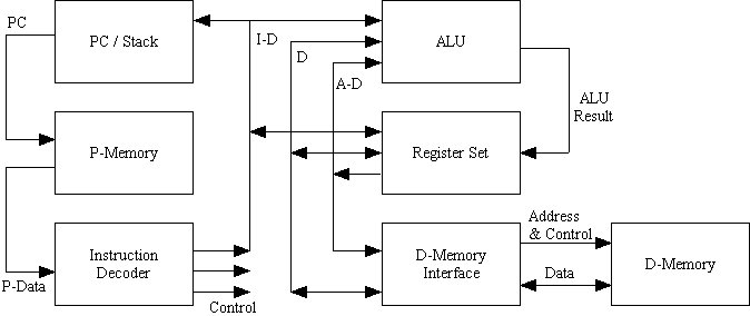
The program counter (PC) is generated and controlled by the PC and stack module. This is used to address the program memory and provide instructions and immediate data for the E-Risc. The PC is always 16 bits wide, as is the data width of the program memory. (Note the PC could shrink if a particular application did not need so much program memory, but it does not grow with the data width of the E-Risc.) This gives 64k words of instruction space and it should be more than enough for the sort of embedded applications the E-Risc is intended. A wait signal can be associated with the program memory to take into account slow memory, or caches.
The data out of the program memory is passed to the instruction decoder. This is the main controller for the whole E-Risc. It sends control to each of the other elements to sequence them. Immediate data from the instruction decoder can pass to the register set, the ALU or the PC/stack via the immediate-data bus (I-D).
The main data flow is to/from the register set. This is a collection of 16 registers, of the appropriate data width (and the shadow registers, see interrupts). The data flow to/from the ALU and data memory are from/to the register set. This uses the data (D) and the address-data (A-D) buses. The PC/stack can also be feed with data from the registers using the I-D bus (this is to implement pointers to functions etc.). The results of the ALU is always fed to a register.
Although it is not implemented in the first generation of the E-Risc
the internal buses are so arranged that the stack could be in data memory,
instead of within the PC/stack. This will probably be added in the near
future. This description is proposing 1.0 in which a number of simplifications
have been made to ease development.
Data Memory Accesses.
Loads and stores are defined having an address and a data width (size).
The size of the load/store is a byte (8 bits), a word (16 bits), a long
(32 bits) or a long long (64 bits). Only the sizes up to the data width
of the processor are supported. The address given is a byte address but
the data widths greater than a byte must be aligned such that the address
of the data is the same as the byte address of the most significant byte
of the data. (We are talking BIG endian...) The data memory interface will
convert the required access to a correct address and one or more of the
control signals for the data memory. For simplicity all reads from data
memory read the whole width of the memory and writes are controlled by
a number write enable signals, one per byte of the data memory. A wait
input is provided so that accesses to slower memories or peripherals can
be performed.
Interrupts.
Single level of interrupts.
When an interrupt request (IRQ) is detected it is past on to the instruction decoder, where it will be held off during a multiple fetch instruction or any change to the program counter. When the interrupt is serviced the program counter is pushed on to the stack and the value from the interrupt handler register is loaded into the program counter. The next instruction loaded is ignored and executed when the interrupt has been handled (we will return to its address). The status register and the lower four registers are switched to an alternative set of shadow registers so the use of them will not corrupt the non interrupt processing. Other registers could be used but they will need to be stored first and then restored before returning from the interrupt.Instruction Support
- Load IRQ handler register.
- Enable IRQ.
- Disable IRQ.
- Return from interrupt.