|
Mutlu ÖZGÜN
ana sayfa
VHDL,AVHDL, Verilog HDL
KODLARI
How to Use VHDL Examples
Altera provides VHDL design examples in two
formats: as downloadable executable files or displayed as
text in your web browser. Click the executable file link to
download the file to your hard disk. To use VHDL examples
that are displayed as text in your Quartus II or MAX+PLUS II
project, you can "copy and paste" the text from your web
browser into the Quartus II or MAX+PLUS II Text Editor. Make
sure that the file name of the VHDL Design File (.vhd)
corresponds to the entity name in the example. For instance,
if the entity name is myram, you should save
the file as myram.vhd.

VHDL: Behavioral Counter
This example implements a behavioral
counter with load, clear, and up/down features. It has not
been optimized for a particular device architecture, so
performance may vary. Altera recommends using the lpm_counter
function to implement a counter . This example is provided
to show counter implementation that does not require the LPM.
counters.vhd
ENTITY counters IS
    PORT(
    	d       : IN    INTEGER RANGE 0 TO 255;
        clk     : IN    BIT;
        clear   : IN    BIT;
        load    : IN    BIT;
        up_down : IN    BIT;
        qd      : OUT   INTEGER RANGE 0 TO 255);
END counters;

ARCHITECTURE a OF counters IS
BEGIN
    -- An up/down counter
    PROCESS (clk)
         VARIABLE    cnt       : INTEGER RANGE 0 TO 255;
         VARIABLE    direction : INTEGER;
    BEGIN
        IF (up_down = '1') THEN  --Generate up/down counter
            direction := 1;
            ELSE
                direction := -1;
        END IF;
            IF (clk'EVENT AND clk = '1') THEN
                IF (load = '1') THEN         --Generate loadable
                    cnt := d;                --counter. Take these
                    ELSE                     --lines out to increase performance.
                    cnt := cnt + direction;
                 END IF;
                --The following lines will produce a synchronous
                --clear on the counter
                  IF (clear = '0') THEN
                     cnt := 0;
                  END IF;
             END IF;
    qd <= cnt;   --Generate outputs
    END PROCESS;
END a;
VHDL: Down Counter
This example is a 4-bit down counter with
a synchronous set. This example shows two different methods
for mapping the lpm_counter function. The
second method, which is commented out in the example, maps
all of the ports on the lpm_counter.
MAX+PLUS II will synthesize out the unused connections.
cnt_3.vhd
LIBRARY ieee;
USE ieee.std_logic_1164.ALL;

LIBRARY lpm;                 --Allows use of all Altera LPM
USE lpm.lpm_components.all;  --functions
ENTITY cnt_3 IS
    PORT (clock : IN STD_LOGIC;
          sset  : IN STD_LOGIC;
          q     : OUT STD_LOGIC_VECTOR(3 DOWNTO 0));
END cnt_3;

ARCHITECTURE lpm OF cnt_3 IS
BEGIN
-- Port map 1
U1: lpm_counter
    GENERIC MAP (lpm_width => 4, lpm_direction => "down")

    PORT MAP (clock => clock, sset => sset,
              q => q);
-- Port map 2
--
--    PORT MAP (data => "0000&p;quuot;, clock => clock, clk_en => '1',
--              cnt_en => '1', updownnn => '0', sload  => '0',
--              sset =>  SSET, sclr ===> '0', aload => '0',
--              aset => '0', aclr  =&aamp;> '0', q => q);

--  These portmaps will produce the sameee results.
--  The second portmap has more connectiiions but
--  the extraneous connections will be sssynthesized out.

END;
VHDL: Cycle-Shared Dual-Port RAM (csdpram)
This example shows the instantiation of
the csdpram function in VHDL. Both inputs are 4
bits wide and are 16 words deep. You can customize these
parameters by changing the LPM_WIDTH and
LPM_WIDTHAD values. If used in a FLEX 10K device,
this function will fit best into the embedded array blocks
of the architecture.
cycle.vhd
LIBRARY ieee;
USE ieee.std_logic_1164.ALL;
LIBRARY altera;
USE altera.maxplus2.ALL;
ENTITY cycle IS
    PORT (dataa    : IN STD_LOGIC_VECTOR(3 DOWNTO 0);
          datab    : IN STD_LOGIC_VECTOR(3 DOWNTO 0);
          addressa : IN STD_LOGIC_VECTOR(3 DOWNTO 0);
          addressb : IN STD_LOGIC_VECTOR(3 DOWNTO 0);
          wea,web  : IN STD_LOGIC;
          clock    : IN STD_LOGIC;
          clockx2  : IN STD_LOGIC;
          qa       : OUT STD_LOGIC_VECTOR(3 DOWNTO 0);
          qb       : OUT STD_LOGIC_VECTOR(3 DOWNTO 0));
END cycle;

ARCHITECTURE lpm OF cycle IS
BEGIN
    U1: csdpram
            GENERIC MAP (LPM_WIDTH => 4, LPM_WIDTHAD => 4, LPM_NUMWORDS => 16)
            PORT MAP (dataa => dataa, datab => datab,
                      addressa => addressa,
                      addressb => addressb, wea => wea,
                      web => web, clock => clock,
                      clockx2 => clockx2, qa => qa,
                      qb => qb);
END;
VHDL: Ripple-Carry Adder
This example illustrates the use of the
For Generate statement to construct a ripple-carry adder
from a full adder function. It also shows how to use a
package definition in the usr_def.vhd design
file. Note that the file usr_def.vhd calls a
full adder from the full_add.vhd file. Also
note that usr_def.vhd must be compiled before
f_add8.vhd is compiled. The ripple-carry adder
shown in this example can be used in designs where the
efficient use of logic resources is more important than
design performance.
f_add8.vhd
LIBRARY altera;
USE altera.maxplus2.carry;

LIBRARY ieee;
USE ieee.std_logic_1164.ALL;

LIBRARY WORK;
USE WORK.usr_def.ALL;

ENTITY f_add8 IS
    PORT(
        x_in    :    IN STD_LOGIC_VECTOR(7 DOWNTO 0);
        y_in    :    IN STD_LOGIC_VECTOR(7 DOWNTO 0);
        c_in    :    IN STD_LOGIC;
        sum     :    OUT STD_LOGIC_VECTOR(7 DOWNTO 0);
        c_out   :    OUT STD_LOGIC);
END f_add8;

ARCHITECTURE struct OF f_add8 IS
SIGNAL im  :    STD_LOGIC_VECTOR(6 DOWNTO 0);
SIGNAL imi :    STD_LOGIC_VECTOR(6 DOWNTO 0);
BEGIN
    c0   : full_add
           PORT MAP (x_in(0),y_in(0),c_in,sum(0),im(0));
    c01  : carry
           PORT MAP (im(0),imi(0));
    c    : FOR i IN 1 TO 6 GENERATE
            c1to6:  full_add PORT MAP (x_in(i),y_in(i),
            imi(i-1),sum(i),im(i));
            c11to16: carry PORT MAP (im(i),imi(i));
           END GENERATE;
    c7   : full_add PORT MAP (x_in(7),y_in(7),
           imi(6),sum(7),c_out);
END struct;
LIBRARY ieee;
USE ieee.std_logic_1164.ALL;
PACKAGE usr_def IS
   COMPONENT full_add
      PORT(
          a      : IN STD_LOGIC;
          b      : IN STD_LOGIC;
          c_in   : IN STD_LOGIC;
          sum    : OUT STD_LOGIC;
          c_out  : OUT STD_LOGIC);
   END COMPONENT;
END usr_def;
LIBRARY ieee;
USE ieee.std_logic_1164.ALL;

ENTITY full_add IS
    PORT(
        a     : IN    STD_LOGIC;
        b     : IN    STD_LOGIC;
        c_in  : IN    STD_LOGIC;
        sum   : OUT   STD_LOGIC;
        c_out : OUT   STD_LOGIC);
END full_add;

ARCHITECTURE behv OF full_add IS
BEGIN
	sum <= a XOR b XOR c_in;
	c_out <= (a AND b) OR (c_in AND (a OR b));
END behv;
VHDL: Converting a Hexadecimal Value to a
Standard Logic Vector
This example shows how to convert a
hexadecimal value to a std_logic_vector. It is
shown in both VHDL '87 (IEEE Std 1076-1987) and VHDL '93 (IEEE
Std 1076-1993).
hex.vhd
LIBRARY ieee;
USE ieee.std_logic_1164.ALL;
USE ieee.std_logic_arith.ALL;

ENTITY hex IS
    PORT(
        D : OUT STD_LOGIC_VECTOR(7 DOWNTO 0));
END hex;

ARCHITECTURE a OF hex IS
BEGIN
-- The following line will convert the hhhex value
-- to a STD_LOGIC_VECTOR in VHDL '87.

    D(7 DOWNTO 0) <= to_stdlogicvector(x"FC");

-- The following line will work in VHDL   '93 (the standard allows
-- this conversion implicitly).
-- D <= x"FC";
END a;
VHDL: Instantiating a DFFE
This example instantiates a D
flipflop with an enable signal (DFFE).
The section that is commented out uses
the same logic, except the IF enable statement
is switched. The commented section will not synthesize
correctly in MAX+PLUS II because the enable
input will feed both the enable on the flipflop
and added combinatorial logic that then feeds the D
input.
simpsig.vhd
ENTITY simpsig IS
    PORT(
        enable  : IN BIT;
        d, clk  : IN BIT;
        q       : OUT BIT
        );
END simpsig;

ARCHITECTURE maxpld OF simpsig IS
BEGIN
    PROCESS(clk)
        BEGIN
            IF (enable = '0' ) then null;
            ELSIF (clk'event and clk = '1') then
            q <= d;
            END IF;
        END PROCESS;
END maxpld;

-- The following implementation is incorrrrect.
-- PROCESS(clk)
--    BEGIN
--        IF (clk'event AND clk = '1') TTTHEN
--            IF (enable = '1' ) THEN
--            q <= d;
--            END IF;
--        END IF;
--    END PROCESS;

-- END maxpld;
VHDL: Creating a Hierarchical Design
This example describes how to create a
hierarchical design using VHDL. The top-level design, called
top.vhd, implements an instance of the function logic.vhd.
In the top.vhd file, a component for the logic function is
declared inside the architecture in which it is
instantiated. The Component Declaration defines the ports of
the lower-level function.
If the two files are in the same
directory, MAX+PLUS® II automatically links the lower-level
design (logic.vhd) to the top-level design (top.vhd). If
not, you must specify the directory where you stored the
lower-level design using the User Libraries command (Options
menu).
top.vhd (Top-level
file)
LIBRARY ieee;
USE ieee.std_logic_1164.ALL;

ENTITY top IS
      PORT(w_in, x_in, y_in	:IN std_logic;
               clock        :IN std_logic;
               z_out        :OUT std_logic);
END top;

ARCHITECTURE a OF top IS

COMPONENT logic
        PORT(a,b,c    :IN std_logic;
              x       :OUT std_logic);
END COMPONENT;

SIGNAL w_reg, x_reg, y_reg, z_reg	:std_logic;

BEGIN
low_logic       : logic PORT MAP (a => w_reg, b => x_reg, c => y_reg, x => z_reg);

PROCESS(clock)
BEGIN
     IF (clock'event AND clock='1') THEN
         w_reg<=w_in;
         x_reg<=x_in;
         y_reg<=y_in;
         z_out<=z_reg;
    END IF;
END PROCESS;

END a;
LIBRARY ieee;
USE ieee.std_logic_1164.ALL;

ENTITY logic IS
      PORT(a,b,c     : IN std_logic;
             x       : OUT std_logic);
END logic;

ARCHITECTURE a OF logic IS
BEGIN
PROCESS (a,b,c)
BEGIN
     x<=(a and b) or c;
END PROCESS;
END;
VHDL: Carry Look-Ahead Adder
This example implements an 8-bit carry
look-ahead adder by recursively expanding the carry term to
each stage. Recursive expansion allows the carry
expression for each individual stage to be implemented in a
two-level AND-OR expression. This reduces the
carry signal propagation delay (the limiting
factor in a standard ripple carry adder) to produce a
high-performance addition circuit.
Altera recommendeds using the
lpm_add_sub function to implement an adder. This
example is provided to show an adder implementation that
does not require the LPM.
This design works best in a FLEX device
compiled using the Fast synthesis style in MAX+PLUS II. To
compile the project using the Fast synthesis style:
-
Choose Global Project Logic Synthesis
(Assign Menu). The Global Project Logic Synthesis
dialog box is displayed.
-
Select Define Sythesis Style.
-
Choose Fast from the Style
drop-down list box.
c_l_addr.vhd
LIBRARY ieee;
USE ieee.std_logic_1164.ALL;

ENTITY c_l_addr IS
    PORT
        (
         x_in      :  IN   STD_LOGIC_VECTOR(7 DOWNTO 0);
         y_in      :  IN   STD_LOGIC_VECTOR(7 DOWNTO 0);
         carry_in  :  IN   STD_LOGIC;
         sum       :  OUT  STD_LOGIC_VECTOR(7 DOWNTO 0);
         carry_out :  OUT  STD_LOGIC
        );
END c_l_addr;

ARCHITECTURE behavioral OF c_l_addr IS

SIGNAL    h_sum              :    STD_LOGIC_VECTOR(7 DOWNTO 0);
SIGNAL    carry_generate     :    STD_LOGIC_VECTOR(7 DOWNTO 0);
SIGNAL    carry_propagate    :    STD_LOGIC_VECTOR(7 DOWNTO 0);
SIGNAL    carry_in_internal  :    STD_LOGIC_VECTOR(7 DOWNTO 1);

BEGIN
    h_sum <= x_in XOR y_in;
    carry_generate <= x_in AND y_in;
    carry_propagate <= x_in OR y_in;
    PROCESS (carry_generate,carry_propagate,carry_in_internal)
    BEGIN
    carry_in_internal(1) <= carry_generate(0) OR (carry_propagate(0) AND carry_in);
        inst: FOR i IN 1 TO 6 LOOP
              carry_in_internal(i+1) <= carry_generate(i) OR (carry_propagate(i) AND carry_in_internal(i));
              END LOOP;
    carry_out <= carry_generate(7) OR (carry_propagate(7) AND carry_in_internal(7));
    END PROCESS;

    sum(0) <= h_sum(0) XOR carry_in;
    sum(7 DOWNTO 1) <= h_sum(7 DOWNTO 1) XOR carry_in_internal(7 DOWNTO 1);
END behavioral;
VHDL: Bidirectional Bus
This example implements an 8-bit bus that
feeds and receives feedback from bidirectional pins.
bidir.vhd
(Tri-state bus implementation)
LIBRARY ieee;
USE ieee.std_logic_1164.ALL;
ENTITY bidir IS
PORT(
bidir : INOUT STD_LOGIC_VECTOR (7 DOWNTO 0);
oe, clk : IN STD_LOGIC;
inp : IN STD_LOGIC_VECTOR (7 DOWNTO 0);
outp : OUT STD_LOGIC_VECTOR (7 DOWNTO 0));
END bidir;
ARCHITECTURE maxpld OF bidir IS
SIGNAL a : STD_LOGIC_VECTOR (7 DOWNTO 0); -- DFF that
stores
-- value from
input.
SIGNAL b : STD_LOGIC_VECTOR (7 DOWNTO 0); -- DFF that
stores
BEGIN -- feedback
value.
PROCESS(clk)
BEGIN
IF clk = '1' AND clk'EVENT THEN -- Creates the
flipflops
a <= inp;
outp <= b;
END IF;
END PROCESS;
PROCESS (oe, bidir) -- Behavioral
representation
BEGIN -- of tri-states.
IF( oe = '0') THEN
bidir <= "ZZZZZZZZ";
b <= bidir;
ELSE
bidir <= a;
b <= bidir;
END IF;
END PROCESS;
END maxpld;
VHDL:Tri-State Buses
This example implements 8 tri-state
buffers by using a WHEN-ELSE clause in an
Architecture Body statement. It does not have a feedback
path, and therefore the output pin my_out is
designated as OUT, instead of INOUT.
This example is similar to the VHDL:
Bidirectional Bus example, except that it does not use a
feedback line.
prebus.vhd
LIBRARY IEEE;
    USE ieee.std_logic_1164.ALL;

ENTITY prebus IS
    PORT(
        my_in  : IN STD_LOGIC_VECTOR(7 DOWNTO 0);
        sel    : IN STD_LOGIC;
        my_out : OUT STD_LOGIC_VECTOR(7 DOWNTO 0));
END prebus;

ARCHITECTURE maxpld OF prebus IS
BEGIN
    my_out <= "ZZZZZZZZ"
    WHEN (sel = '1')
    ELSE my_in;
END maxpld;
VHDL: Instantiating a D Flipflop using
lpm_dff
This example instantiates an 8-bit-wide
D flipflop using the lpm_dff
function. The Port Map maps the pins in this instance of the
function to the correspnding ports in the Component
Instantiation Statement for the lpm_dff
function, which is contained in the lpm_component
package.
testdff.vhd
LIBRARY ieee, lpm;
USE ieee.std_logic_1164.ALL;
USE lpm.lpm_components.ALL;

ENTITY testdff IS
    PORT (inputs : IN STD_LOGIC_VECTOR(7 DOWNTO 0);
          clk  : IN STD_LOGIC;
          aset : IN STD_LOGIC ;
          aclr : IN STD_LOGIC ;
          sset : IN STD_LOGIC ;
          sclr : IN STD_LOGIC ;
          en   : IN STD_LOGIC ;
          outputs : OUT STD_LOGIC_VECTOR(7 DOWNTO 0));
END testdff;

ARCHITECTURE dff8 OF testdff IS
BEGIN
    U1 : lpm_ff
            GENERIC MAP(lpm_width => 8)
                PORT MAP(data => inputs,
                clock => clk,q => outputs,
                aclr => aclr, enable => en,
                aset => aset, sset => sset,
                sclr => sclr);
END;
VHDL: ZBT SRAM Controller
Zero bus turnaround™ (ZBT®)
SRAM with No Bus Latency (NoBL™) memory is a
synchronous burst SRAM with a simplified interface that
fully uses the available bandwidth. ZBT SRAM devices use the
full bandwidth because they do not require turnaround
cycles-i.e., idle cycles between read and write operations.
In contrast, standard synchronous burst SRAMs require
turnaround cycles, which significantly reduces the available
bandwidth.
You can implement the Altera®
ZBT SRAM controller reference design in an APEX™ II
device to provide a simplified interface to ZBT SRAM. The
reference design includes VHDL source files, synthesis and
place and route project files, and functional and timing
simulation environments.
ZBT SRAM Controller
System Level Block Diagram

AHDL: Cycle-Shared Dual-Port RAM (csdpram)
This example implements a dual-port RAM
block with two inputs that are 4 bits wide and 16 words
deep. You can change the width (LPM_WIDTH) and
depth (LPM_WIDTHAD) parameters as needed for
your design. The ports of the LPM function are defined in a
Function Prototype Statement (shown in blue text). An
Instance Declaration (shown in red text) implements an
instance of the function.
If you are using this function in a
FLEX 10K design, MAX+PLUS II will implement the RAM in
embedded array blocks (EABs).
csram.tdf
FUNCTION csdpram (dataa[3..0], datab[3..0], addressa[3..0],
                 addressb[3..0], wea, web, clock,clockx2)
   WITH (LPM_WIDTH = 4, LPM_WIDTHAD = 4)
   RETURNS (qa[3..0], qb[3..0], busy);

SUBDESIGN csram
(
   dataa[3..0]         :   INPUT;
   datab[3..0]         :   INPUT;
   addressa[3..0]      :   INPUT;
   addressb[3..0]      :   INPUT;
   qa[3..0]            :   OUTPUT;
   qb[3..0]            :   OUTPUT;
   wea                 :   INPUT;
   web                 :   INPUT;
   clock               :   INPUT;
   clockx2             :   INPUT;
)

VARIABLE
   csdpramtest         :   csdpram;
BEGIN
   csdpramtest.clock = clock;
   csdpramtest.clockx2 = clockx2;
   csdpramtest.dataa[3..0] = dataa[3..0];
   csdpramtest.datab[3..0] = datab[3..0];
   csdpramtest.addressa[3..0] = addressa[3..0];
   csdpramtest.addressb[3..0] = addressb[3..0];
   csdpramtest.wea=wea;
   csdpramtest.web=web;

   qa[3..0]=csdpramtest.qa[3..0];
   qb[3..0]=csdpramtest.qb[3..0];


END;
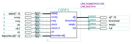
AHDL: Cycle-Shared FIFO (csfifo)
This example implements a cycle-shared
FIFO with 256 8-bit words. The size of the FIFO is defined
with the parameters LPM_WIDTH and
LPM_WIDTHAD. This example uses an Include Statement
(shown in blue text) to import the contents of the Include
File containing the Function Prototype for the csfifo
function. An Instance Declaration (shown in red text)
implements an instance of the function.
If you are using this function in a
FLEX 10K design, MAX+PLUS II will implement the FIFO in
embedded array blocks (EABs).
fifo.tdf
INCLUDE "csfifo.inc";

SUBDESIGN fifo
(
   dataf[7..0]       : INPUT;
   qf[7..0]          : OUTPUT;

   wreq              : INPUT;
   rreq              : INPUT;

   clk               : INPUT;
   clk2              : INPUT;
   clr               : INPUT;

   threshlevel[7..0] : INPUT;
   empty             : OUTPUT;
   full              : OUTPUT;
   threshold         : OUTPUT;
)

VARIABLE

   vxififo           : csfifo
      WITH (LPM_WIDTH = 8, LPM_NUMWORDS = 256);

BEGIN
   -- Input definition for VXI FIFO

   vxififo.clock = clk;
   vxififo.clockx2 = clk2;
   vxififo.clr = clr;

   vxififo.data[7..0] = dataf[7..0];

   vxififo.threshlevel[7..0] = threshlevel[7..0];
   vxififo.wreq = wreq;
   vxififo.rreq = rreq;

   qf[7..0] = vxififo.q[7..0];

   threshold = vxififo.threshold;
   empty = vxififo.empty;
   full = vxififo.full;

END;
AHDL: Parameterized Counter (lpm_counter)
This example implements a parameterized
counter that decodes two values. You can change the width (LPM_WIDTH),
direction (LPM_DIRECTION), and modulus (LPM_MODULUS)
parameters as needed for your design. The eq 11
port is used to decode when the counter reaches 11. AHDL
operators are used to decode when the counter reaches 50
because only 16 eq ports are available in the
lpm_counter function. After the counter reaches
99, it will return to zero. This example uses an Include
Statement (shown in blue text) to import the contents of the
Include File containing the Function Prototype for of the
lpm_counter function. An Instance Declaration
(shown in red text) implements an instance of the function.
upcnt99.tdf
INCLUDE "lpm_counter.inc";

SUBDESIGN upcnt99
(
    clkena, cntena, clr, load, clk, data[7..0]
        : INPUT;
    eleven, fifty
        : OUTPUT;
)

VARIABLE
-- Declare my_count as an 8-bit up counttter with a
-- modulus of 100 (i.e., count to 99)

    my_count : lpm_counter WITH (LPM_WIDTH = 8,
               LPM_DIRECTION = "UP",
               LPM_MODULUS = 100);

BEGIN
-- Connect the data, aclr, clock, clock   enable, synchronous load,
-- and count enable ports. You must connnnect all ports that are used
-- to pins:

   my_count.data[] = data[];
   my_count.aclr = clr;
   my_count.clock = clk;
   my_count.clk_en = clkena;
   my_count.cnt_en = cntena;
   my_count.sload = load;

-- To indicate a 1 at the output (or decccode) when the counter
-- reaches state 11, use the following:
   eleven = my_count.eq11;

-- When the counter reaches 12, the outppput goes back to 0
-- Decode fifty.
   IF (my_count.q[] == 50) THEN
      fifty = VCC;
   END IF;
END;
AHDL: Parameterized Tri-State Bus (lpm_bustri)
This example implements a tri-state bus.
The width of the bus is specified with the LPM_WIDTH
parameter and can be changed for your design. The dq
and data_out pins are fed by tri-state buses.
Because tri-state buses cannot feed internal logic, you
should use the lpm_bustri function only if
dq and data_out feed pins. This
example uses an Include Statement (shown in blue text) to
import the contents of the Include File containing the
Function Prototype of the lpm_bustri function.
An Instance Declaration implements (shown in red text) an
instance of the function.
tribus.tdf
INCLUDE "lpm_bustri";

SUBDESIGN tribus
(
   enable_out, enable_in  : INPUT;
   datain[7..0]           : INPUT;
   dataout[7..0]          : OUTPUT;
   dq[7..0]               : BIDIR;
)

VARIABLE

   u1 : lpm_bustri
        WITH (LPM_WIDTH=8);

BEGIN

   u1.data[7..0] = datain[7..0];
   u1.enabletr = enable_out;
   u1.enabledt = enable_in;
   dataout[7..0] = u1.result[7..0];
   dq[7..0] = u1.tridata[7..0];

END;
AHDL: Creating a Hierarchical Design
This example describes how to create a
hierarchical design using AHDL. This design is identical to
the VHDL and schematic hierarchy examples. The file
top.tdf is the top level, which calls the two lower
level files bottom1.tdf and bottom2.tdf.
The files bottom1.inc and bottom2.inc
must be created for the lower level files so that they can
be instantiated into the top level. When the project is set
to either bottom1.tdf or bottom2.tdf,
you can create bottom1.inc and
bottom2.inc by choosing Create Default Include File
(File menu) in MAX+PLUS II. This step creates the Include
Files needed by the top-level AHDL file.
top.tdf
INCLUDE "bottom1";    --File bottom1.inc contains function prototype
                      --of bottom1.tdf
INCLUDE "bottom2";    --File bottom2.inc contains function prototype
                      --of bottom2.tdf

SUBDESIGN top
(
q,p,r   : INPUT;
z       : OUTPUT;
)

VARIABLE
u1    : bottom1;    --Instantiates bottom1.tdf
                    --The same TDF can be instantiated multiple times
u2    : bottom2;    --Instantiates bottom2.tdf

BEGIN
u1.a = q;           --These lines connect the ports
u1.b = p;           --or the u1 and u2 instantiations.
u2.l = u1.c;
u2.m = r;
z = u2.n;
END;
SUBDESIGN bottom1
(
a,b    : INPUT;
c      : OUTPUT;
)

BEGIN
    c = a AND b;
END ;
SUBDESIGN bottom2
(
l,m    : INPUT;
n      : OUTPUT;
)

BEGIN
    n = l OR m;
END ;
bottom1.inc
-- Copyright (c) Altera Corporation,
1996. This file may contain
proprietary and confidential -- information of Altera
Corporation that may be used, copied, and
disclosed only pursuant to -- the terms of Altera's
Program License Agreement. Altera makes no
claim to any end-user or -- third-party proprietary
information that also may be contained in
this file. This notice -- must be contained as part of
this text at all times.
-- MAX+plus II Include File -- Version
7.0 08/21/96 -- Created: Tue Sep 17 11:00:22 1996 FUNCTION
bottom1 (a, b) RETURNS (c);
bottom2.inc
-- Copyright (c) Altera Corporation, 1996. This file may contain
   proprietary and confidential
-- information of Altera Corporation thaaat may be used, copied, and
   disclosed only pursuant to
-- the terms of Altera's Program Licenseee Agreement. Altera makes no
   claim to any end-user or
-- third-party proprietary information ttthat also may be contained in
   this file. This notice
-- must be contained as part of this texxxt at all times.

-- MAX+plus II Include File
-- Version 7.0 08/21/96
-- Created: Tue Sep 17 11:00:04 1996

FUNCTION bottom2 (l, m)
    RETURNS (n);
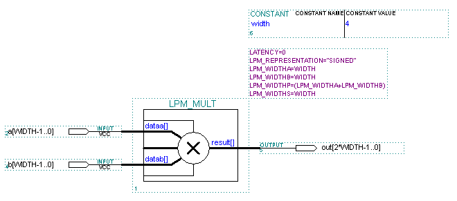
AHDL: Parameterized Multiplier (lpm_mult)
This example uses the lpm_mult
function and a constant to implement a parameterized
multiplier that multiplies two 4-bit values. You can adjust
the size of the multiplier by changing the value of the
constant WIDTH. This example uses an Include
Statement (shown in blue text) to import the contents of the
Include File containing the Function Prototype for the
lpm_mult function. An Instance Declaration (shown in
red text) implements an instance of the function.
tmul3t.tdf
CONSTANT WIDTH = 4;

INCLUDE "lpm_mult.inc";

SUBDESIGN tmul3t
(
    a[WIDTH-1..0]      : INPUT;
    b[WIDTH-1..0]      : INPUT;
    out[2*WIDTH-1..0]  : OUTPUT;
)

VARIABLE

    mult : lpm_mult WITH (LPM_REPRESENTATION="SIGNED",
                 LPM_WIDTHA=WIDTH,LPM_WIDTHB=WIDTH,
                 LPM_WIDTHS=WIDTH,LPM_WIDTHP=WIDTH*2);

BEGIN
    mult.dataa[] = a[];
    mult.datab[] = b[];
    out[] = mult.result[];
END;
AHDL: Parameterized Multiplexer (lpm_mux)
In this example, four 4-bit-wide buses (a,
b, c, and d) are
multiplexed. The widths of the four buses are specified with
the parameter LPM_WIDTH, the number of buses
being multiplexed is specified with LPM_SIZE,
and the number of select lines is specified with
LPM_WIDTHS. You can change any of these parameters to
suit the needs of your design. The ports of the LPM function
are defined in a Function Prototype Statement (shown in blue
text). An Instance Declaration (shown in red text)
implements an instance of the function.
mux.tdf
FUNCTION lpm_mux (data[LPM_SIZE-1..0][LPM_WIDTH-1..0],
   sel[LPM_WIDTHS-1..0])
      WITH (LPM_WIDTH, LPM_SIZE, LPM_WIDTHS, CASCADE_CHAIN)
      RETURNS (result[LPM_WIDTH-1..0]);

SUBDESIGN mux
(
   a[3..0], b[3..0], c[3..0], d[3..0]  : INPUT;
   select[1..0]                        : INPUT;

   result[3..0]                        : OUTPUT;
)

BEGIN

result[3..0] = lpm_mux (a[3..0], b[3..0], c[3..0], d[3..0],
   select[1..0])
      WITH (LPM_WIDTH=4, LPM_SIZE=4, LPM_WIDTHS=2);

END;
AHDL: Parameterized RAM with Separate Input
& Output Ports (lpm_ram_dq)
This example implements a RAM block with
256 32-bit words. This design fits in 4 FLEX 10K embedded
array blocks (EABs), with each EAB containing 8 bits of the
total word. This example uses an Include Statement (shown in
blue text) to import the contents of the Include File
containing the Function Prototype of the lpm_ram_dq
function. An Instance Declaration (shown in red text)
implements an instance of the function.
ram_dq.tdf
INCLUDE "lpm_ram_dq.inc";

SUBDESIGN ram_dq
(
   clk                : INPUT;
   we                 : INPUT;
   ram_data[31..0]    : INPUT;
   ram_add[7..0]      : INPUT;

   data_out[31..0]    : OUTPUT;
)

BEGIN

data_out[31..0] = lpm_ram_dq (ram_data[31..0], ram_add[7..0], we, clk, clk)
      WITH (LPM_WIDTH=32, LPM_WIDTHAD=8);

END;
AHDL: Tri-State Buses Connected to a
Bidirectional Bus
This example implements an 8-bit bus that
feeds and receives feedback from bidirectional pins. The
example contains 8 D-type flipflops, or DFFs, (named
a[7..0]), which store the values of the inputs. The
DFFs named b[7..0] store the data from the
feedback line.
This example can be implemented in two
ways, both of which are shown below. In the first method,
the tri-state buses are declared in the VARIABLE
section; the second method uses in-line references to create
the tri-state buses.
Method 1: tri_bb.tdf
-- This method declares the tri-state buses
-- in the VARIABLE section.

SUBDESIGN tri_bb
(
    inp[7..0], oe, clk  : INPUT;
    outp[7..0]          : OUTPUT;
    bidirp[7..0]        : BIDIR;
)

VARIABLE
    my_tri[7..0]      : TRI;
    a[7..0], b[7..0]  : DFF;

BEGIN
-- Connect the a[7..0] flipflops
    a[].clk = clk;
    a[].d = inp[];
    my_tri[].in = a[].q;

-- Connect the b[7..0] flipflops
    b[].clk = clk;
    b[].d = bidirp[];
    outp[] = b[].q;

-- Connect the tri-state buffers
    my_tri[].oe = oe;
    bidirp[] = my_tri[].out;
Method 2: tri_bb.tdf
-- This method uses in-line references to create
-- tri-state buses.

SUBDESIGN tri_bb
(
    inp[7..0], oe, clk  : INPUT;
    outp[7..0]          : OUTPUT;
    bidirp[7..0]        : BIDIR;
)

VARIABLE
   a[7..0], b[7..0] : DFF;

BEGIN
   a[7..0].clk = clk;
   b[7..0].clk = clk;

   a[7..0].d = inp[7..0];
   b[7..0].d = bidirp[7..0];

   bidirp[0] = TRI(a[0].q, oe);
   bidirp[1] = TRI(a[1].q, oe);
   bidirp[2] = TRI(a[2].q, oe);
   bidirp[3] = TRI(a[3].q, oe);
   bidirp[4] = TRI(a[4].q, oe);
   bidirp[5] = TRI(a[5].q, oe);
   bidirp[6] = TRI(a[6].q, oe);
   bidirp[7] = TRI(a[7].q, oe);

   outp[7..0] = b[7..0].q;
END;
AHDL: Tri-State Buses Converted to a
Multiplexer
In this example, three tri-state buses
feed a flipflop. Because Altera devices do not have internal
device tri-state buses (i.e., tri-state buffers only exist
in I/O cells), MAX+PLUS II converts the tri-state bus to a
multiplexer.
tribus.tdf
SUBDESIGN tribus
(
   ina[7..0], inb[7..0], inc[7..0], oe_a, oe_b, oe_c, clock
               : INPUT;
   out[7..0]   : OUTPUT;
)

VARIABLE
   tri_a[7..0], tri_b[7..0], tri_c[7..0] : TRI;
   mid[7..0]                             : TRI_STATE_NODE;
   flip[7..0]                            : DFF;

BEGIN
-- Declare the data inputs to the tri-stttate buses
   tri_a[] = ina[];
   tri_b[] = inb[];
   tri_c[] = inc[];

-- Declare the output enable inputs to ttthe tri-state buses
   tri_a[].oe = oe_a;
   tri_b[].oe = oe_b;
   tri_c[].oe = oe_c;

-- Connect the outputs of the tri-state   buses together
   mid[] = tri_a[];
   mid[] = tri_b[];
   mid[] = tri_c[];

-- Feed the output pins
   flip[].d = mid[];
   flip[].clk = clock;
   out[] = flip[].q;
END;
Problem
Are the SXT
and EXT functions supported by MAX+PLUS® II
VHDL?
Solution
The SXT and EXT
functions are used for sign extension and zero extension,
respectively, for signals of the type STD_LOGIC_VECTOR.
Although these functions are listed in the
ieee.std_logic_arith library package, they are not supported
by MAX+PLUS II VHDL.
To perform these functions, you can use
VHDL code and a component declaration. The code for both
sign-extension and zero-extension functions and their
component declarations is shown below. Generics are used to
specify the width of the input and output vectors.
The following is the code for the
sign-extension function:
LIBRARY ieee;
USE ieee.std_logic_1164.ALL;
USE ieee.std_logic_arith.ALL;

ENTITY sign_ext IS
  GENERIC( WIDTH_IN : INTEGER := 4; SIZE_OUT : INTEGER := 8);
  PORT(
    d_in  : IN  STD_LOGIC_VECTOR(WIDTH_IN-1 DOWNTO 0);
    d_out : OUT STD_LOGIC_VECTOR(SIZE_OUT-1 DOWNTO 0) );
END sign_ext;

ARCHITECTURE behavior OF sign_ext IS

BEGIN
  PROCESS(d_in)
    VARIABLE zero: BOOLEAN;
  BEGIN
    IF (d_in(WIDTH_IN-1) = '0') THEN
      zero := true;
    ELSE
      zero := false;
    END IF;

    FOR j IN WIDTH_IN TO (size_out-1) LOOP
      IF (zero) THEN
        d_out(j) <= '0';
      ELSE
        d_out(j) <= '1';
      END IF;
    END LOOP;

    d_out(WIDTH_IN-1 DOWNTO 0) <= d_in(WIDTH_IN-1 DOWNTO 0);
    END PROCESS;
END behavior;
The component declaration for the
sign-extension function is shown below:
COMPONENT sign_ext
  GENERIC (WIDTH_IN: INTEGER; SIZE_OUT: INTEGER);
  PORT (
    d_in: IN STD_LOGIC_VECTOR(WIDTH_IN-1 DOWNTO 0);
    d_out: OUT STD_LOGIC_VECTOR(SIZE_OUT-1 DOWNTO 0) );
END COMPONENT;
The code for the zero-extension function
is shown below:
LIBRARY ieee;
USE ieee.std_logic_1164.all;
USE ieee.std_logic_arith.all;

ENTITY zero_ext IS
	GENERIC( WIDTH_IN : INTEGER := 4; SIZE_OUT : INTEGER := 8);
	PORT(
	d_in 	:	IN	STD_LOGIC_VECTOR(WIDTH_IN-1 DOWNTO 0);
	d_out	:	OUT	STD_LOGIC_VECTOR(SIZE_OUT-1 DOWNTO 0));
END ZERO_EXT;

ARCHITECTURE behavior OF zero_ext IS
BEGIN
	PROCESS(d_in)
   	BEGIN
	FOR j IN width_in TO size_out-1 LOOP
		d_out(j) <= '0';
	END LOOP;
	d_out(WIDTH_IN-1 DOWNTO 0) <= d_in(WIDTH_IN-1 DOWNTO 0);
 	END PROCESS;
END behavior;
The component declaration for the
zero-extension function is specified below:
COMPONENT zero_ext
   GENERIC (	WIDTH_IN: INTEGER;
      		SIZE_OUT: INTEGER);
   PORT (d_in: IN STD_LOGIC_VECTOR(WIDTH_IN-1 DOWNTO 0);
   	d_out: OUT STD_LOGIC_VECTOR(SIZE_OUT-1 DOWNTO 0));
END COMPONENT;
Verilog HDL: Behavioral Counter
This example describes an 8-bit loadable
counter with count enable. The always
construct, highlighted in red text, describes how the
counter should behave.
behav_counter.v
module behav_counter( d, clk, clear, load, up_down, qd);

// Port Declaration

input   [7:0] d;
input   clk;
input   clear;
input   load;
input   up_down;
output  [7:0] qd;

reg     [7:0] cnt;


assign qd = cnt;


always @ (posedge clk)
begin
    if (!clear)
        cnt = 8'h00;
    else if (load)
        cnt = d;
    else if (up_down)
        cnt = cnt + 1;
    else
        cnt = cnt - 1;
end

endmodule
Verilog HDL: Bidirectional Pin
This example implements a clocked
bidirectional pin in Verilog HDL. The value of OE
determines whether bidir is an input, feeding
in inp, or a tri-state, driving out the value
b.
bidir.v
module bidirec (oe, clk, inp, outp, bidir);

// Port Declaration

input   oe;
input   clk;
input   [7:0] inp;
output  [7:0] outp;
inout   [7:0] bidir;

reg     [7:0] a;
reg     [7:0] b;

assign bidir = oe ? a : 8'bZ ;
assign outp  = b;

// Always Construct

always @ (posedge clk)
begin
	b <= bidir;
	a <= inp;
end

endmodule
Verilog HDL: Creating a Hierarchical Design
This example describes how to create a
hierarchical design using Verilog HDL. This design is
identical to the VHDL, AHDL and schematic hierarchy
examples. The file top_ver.v is the top level,
which calls the two lower level files bottom1.v
and bottom2.v.
vprim.v
top_ver.v
module top_ver (q, p, r, out);
input q, p, r;
output out;
reg out, intsig;
bottom1 u1(.a(q), .b(p), .c(intsig));
bottom2 u2(.l(intsig), .m(r), .n(out));
endmodule
bottom1.v
module bottom1(a, b, c);

input     a, b;
output     c;
reg      c;

always
begin
     c<=a & b;
end

endmodule
bottom2.v
module bottom2(l, m, n);

input     l, m;
output    n;
reg       n;

always
begin
     n<=l | m;
end
endmodule
Verilog HDL: Parameterized Counter
This example shows how to instantiate an
LPM function in Verilog HDL. In this case, an
LPM_COUNTER is instantiated using the aclr,
clock, and q ports. The parameter
values are set with the keyword defparam, as
shown in red text. Both the port mapping and the parameter
names are referred to by the period (.) operator after the
variable name. In this case, the variable is u1.
check_lpm.v
module check_lpm ( clk, reset, q);
// Port Declaration

input   clk;
input   reset;
output  [7:0] q;

lpm_counter u1 (.aclr(reset), .clock(clk), .q(q));
defparam u1.lpm_width= 8;
defparam u1.lpm_direction= "UP";

endmodule
Verilog HDL: Instantiating a DFFE
This example describes how to generate a
D flipflop with enable (DFFE) behaviorally with asynchronous
preset and reset signals. Both the preset and reset signals
are active low, controlling the output of the DFFE whenever
either signal goes low.
dffeveri.v
module dffeveri (q, d, clk, ena, rsn, prn);

// port declaration

input   d, clk, ena, rsn, prn;
output  q;
reg     q;

always @ (posedge clk or negedge rsn or negedge prn) begin

//asynchronous active-low preset
    if (~prn)
        begin
        if (rsn)
            q = 1'b1;
        else
            q = 1'bx;
        end

//asynchronous active-low reset
     else if (~rsn)
        q = 1'b0;

//enable
     else if (ena)
		q = d;
end

endmodule
Verilog HDL: Instantiating MAX+PLUS II
Primitives
This example describes how to instantiate
MAX+PLUS II primitives in Verilog HDL. It instantiates a
simple D-type flip-flop, an LCELL primitive, and an
open-drain pin.
vprim.v
module vprim (indata, outdata, clock);

input      indata, clock;
output     outdata;
reg        out_dff, out_lcell;

dff     d1(.d(indata), .q(out_dff), .clk(clock));
lcell   l1(.in(out_dff), .out(out_lcell));
opndrn  o1(.in(out_lcell), .out(outdata));

endmodule
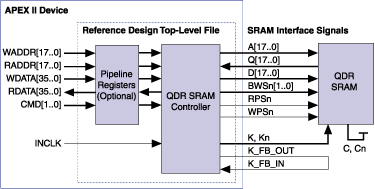
Verilog HDL: QDR SRAM Controller
The QDR Consortium designed the quad data
rate (QDR) SRAM architecture for high-performance
communications systems such as routers and ATM switches. QDR
SRAMs can handle the transfer of four data words through the
SRAM in a single clock cycle.
You can implement the Altera®
QDR SRAM controller reference design in an APEX™ II
device to provide a simplified interface to a QDR SRAM
device. The reference design includes Verilog HDL source
files, synthesis, and place and route project files, and
functional and timing simulation environments.
QDR SRAM Controller
Top-Level Block Diagram
Verilog HDL: Parameterized RAM with
Separate Input & Output Ports
This example shows how to instantiate a
memory block using the LPM function lpm_ram_dq.
The variable ram uses the lpm_ram_dq
function from the LPM library. The ports are initially
defined and then mapped to the LPM ports, as shown in red
text. The parameter values are then passed through with the
keyword defparam. In this example, a 16 x 256
RAM block is instantiated; you can use a similar process to
instantiate RAM blocks of other sizes.
The lpm_file parameter refers
to the Memory Initialization File (.mif) that
specifies the initial content of a memory block (RAM or
ROM). An MIF is an ASCII text file can be created manually
or saved from the output of a simulation. In an MIF, you are
required to specify the memory depth and width values and
optionally you can specify the radixes used to display and
interpret addresses and data values. These values are shown
in red text in the extract from the sample file,
map_lpm_ram.mif, which is included below. An MIF is used
as an input file for memory initialization in the
MAX+PLUS II Compiler and Simulator.
RAMveri.v
// instantiation of lpm_ram_dq, 16-bit data, 256 address location

module map_lpm_ram (dataout, datain, addr, we, inclk, outclk);

// port instantiation

input   [15:0] datain;
input   [7:0] addr;
input   we, inclk, outclk;

output  [15:0] dataout;

// instantiating lpm_ram_dq

lpm_ram_dq ram (.data(datain), .address(addr), .we(we), .inclock(inclk),
				.outclock(outclk), .q(dataout));

// passing the parameter values

defparam ram.lpm_width = 16;
defparam ram.lpm_widthad = 8;
defparam ram.lpm_indata = "REGISTERED";
defparam ram.lpm_outdata = "REGISTERED";
defparam ram.lpm_file = "map_lpm_ram.mif";

endmodule
Extract from the MIF file
WIDTH = 16;
DEPTH = 256;

ADDRESS_RADIX = HEX;
DATA_RADIX = HEX;

CONTENT BEGIN
   0   :   ffff;
   1   :   0000;
   2   :   bbf3;
   3   :   0000;
   4   :   0000;
   .
   .
   .
   fb   :   0000;
   fc   :   0000;
   fd   :   0000;
   fe   :   0000;
   ff   :   0000;
END;
Verilog HDL: Synchronous State Machine
This is a Verilog example that shows the
implementation of a state machine. The first CASE
statement defines the outputs that are dependent on the
value of the state machine variable state. The second
CASE statement defines the transitions of state
machine and the conditions that control them.
statem.v
module statem(clk, in, reset, out);

input clk, in, reset;
output [3:0] out;

reg [3:0] out;
reg [1:0] state;

parameter zero=0, one=1, two=2, three=3;

always @(state)
     begin
          case (state)
               zero:
                    out = 4'b0000;
               one:
                    out = 4'b0001;
               two:
                    out = 4'b0010;
               three:
                    out = 4'b0100;
               default:
                    out = 4'b0000;
          endcase
     end

always @(posedge clk or posedge reset)
     begin
          if (reset)
               state = zero;
          else
               case (state)
                    zero:
                         state = one;
                    one:
                         if (in)
                              state = zero;
                         else
                              state = two;
                    two:
                         state = three;
                    three:
                         state = zero;
               endcase
     end

endmodule
Verilog HDL: Tri-State Instantiation
This simple example shows how to
instantiate a tri-state buffer in Verilog HDL using the
keyword bufif1. The output type is tri.
The buffer is instantiated by bufif1 with the
variable name b1.
tristate.v
module Tristate (in, oe, out);

	input   in, oe;
	output  out;
	tri     out;

	bufif1  b1(out, in, oe);

endmodule
How to Use Graphic Editor Examples
Graphic Editor examples contain links to a
downloadable Graphic Design Files (.gdf). To use
these examples, perform the following steps:
-
Click on the download link with the
right mouse button choose Save Link As from the
pop-up menu.
-
Save the file to your hard disk.
-
Open the file in MAX+PLUS II.
Graphic Editor: Cycle-Shared Dual-Port RAM
(csdpram)
This example implements a dual-port RAM
block with two inputs that are 4 bits wide and 16 words
deep. You can change the width (LPM_WIDTH) and
depth (LPM_WIDTHAD) parameters as needed for
your design.
If you are using this function in a
FLEX 10K design, MAX+PLUS II can implement the RAM in
embedded array blocks (EABs).
cycle.gdf

Graphic Editor: Cycle-Shared First-In
First-Out (FIFO) Function (csfifo)
This example implements a cycle-shared
first-in first-out (FIFO) function with 256 8-bit words. The
size of the FIFO function is defined with the
LPM_WIDTH and LPM_WIDTHAD parameters .
If you are using this function in a FLEX 10K design,
MAX+PLUS II can implement the RAM in embedded array blocks
(EABs).
z_fifo.gdf
Graphic Editor: Parameterized Multiplier (lpm_mult)
This example uses the lpm_mult
function and a constant to implement a parameterized
multiplier that multiplies two 4-bit values. You can adjust
the size of the multiplier by changing the value of the
WIDTH constant.
tmul3.gdf
Graphic Editor:
Parameterized Multiplexer (lpm_mux)
In this example, four 4-bit-wide buses (a,
b, c, and d) are
multiplexed. The widths of the four buses are specified with
the LPM_WIDTH parameter, the number of buses
being multiplexed is specified with LPM_SIZE,
and the number of select lines is specified with
LPM_WIDTHS. You can change any of these parameters to
suit the needs of your design.
gdfmux.gdf

Graphic Editor: Parameterized Tri-State Bus
(lpm_bustri)
This Graphic Editor example implements a
parameterized tri-state bus. The width of the bus is
specified with the LPM_WIDTH parameter and can
be modified in your design. The dq and
data_out pins are fed by tri-state buffers. Because
tri-state buses cannot feed internal logic, the dq
and data_out pins will be converted into
multiplexers if they feed internal logic.
tribus.gdf

Graphic Editor: Tri-State Buses Converted
to a Multiplexer
In this example, three tri-state buses
feed a flipflop. Because Altera devices do not have internal
device tri-state buses (i.e., tri-state buffers only exist
in I/O cells), MAX+PLUS II converts the tri-state bus to a
multiplexer.
tri_bus.gdf


|