
Electrical and
Electronic Engineering
Solid State Digital Recorder
O.C.Au
BEng (Hons)Degrees in Electronic and
Computer Engineering 1995/1996
Contents
1. Introduction
It is becoming common in many fields to contrast or compare analog and digital quantities. Thus, in the field of measurements, digital indicating instruments are being increasingly used to display readings. Analog data transmission and digital data transmission are competing in the field of communications etc., but the very existence of this competition is linked to the possibility of passing from an analog signal to its digital equivalent or vice versa, and these operations assume converters to be available.
Before examining the various analog to d igital (A-D) and digital to analog (D-A) conversion processes it is useful to review the properties of each type of representation; in particular this may help select the representation most suited to the problem at hand.
An analog signal is a signal whose value varies continuously with time, its instantaneous amplitude itself varying continuously within a limited range. The simplest example is that of a sinusoidal signal Asin(w t + f ), whose instantaneous value covers all the values within the range (-A, +A). An analog signal may very often be expressed as a weighted sum of sinusoidal signals.
The analog signal is a simple type of signal which can quite conveniently be transmitted, but its simplicity results in several drawbacks. It is sensitive to parasitic signals and its amplitude or phase can be distorted by the transmitting system. When it undergoes such operations as analog multiplication the accuracy with which the signal is known is often reduced. Moreover it is difficult to store an analog signal.
On the other hand a digital signal usually appears as a series of symbols. Thus, in a binary system a signal consists of a series of numbers, each of which is 0 or 1, that may be given physical form by the absence or presence of pulses. It can be said that the signal is represented by a word of a given format that is of a given structure. The digital signal represents the value of a quantity at a specific instant. It is not a continuous signal and since the symbols making up this signal (usually numbers) can only vary by 'steps' the value represented by the signal must, perforce, be discrete.
These difference from the analog signal, which may appear to be obstacles, are largely compensated by the advantages gained by the digital representation. First of all a digital signal is far less sensitive to the imperfections of the transmitting system (distortion, noise) since it is only necessary to detect the pulses in order to obtain the information, their precise characteristics (amplitude, duration) not being taken into account. During the various operations the accuracy of the signal is maintained (if some of the truncating that is sometimes carried out is ignored). On the other hand the pass band required for transmitting digital information is much greater than the pass band needed for an analog representation of the information.
Thus, each representation has its advantages and disadvantages; the choice of one or other method must take into account the nature of the signal available, the possibility of introducing a digital process, the likelihood of transmitting the information, etc.
Information processing systems may be divided into analog systems and digital systems. In the first case the systems handle signals that vary in a continuous way whereas in the second case the systems handle discrete variables called digital numbers. Any digital treatment of an analog signal first requires an analog to digital conversion operation. If it is desired to recover the processed information in its initial analog form then the inverse conversion operation is needed.
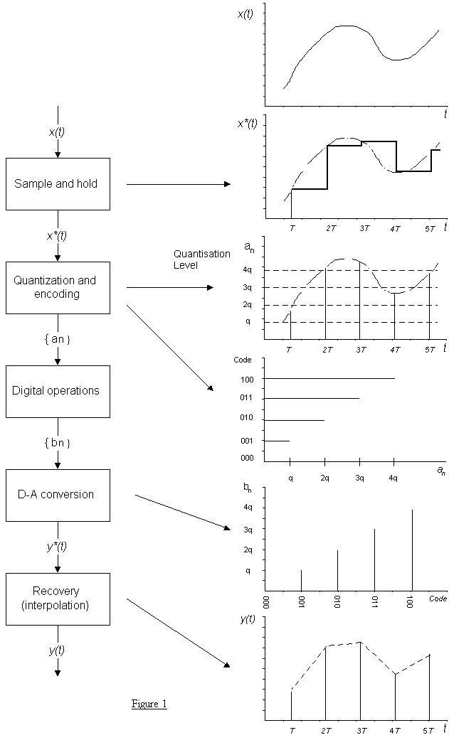
It is necessary now to examine in some detail the operations required by the conversion processes. Let x(t) represent a given analog signal and let x*(t) be the series of discrete values of the given signal taken at regular time intervals of period Te. The operation which allows the change from x(t) to x*(t) is the sampling operation. Thus in an analog to digital conversion process a series of numbers {an} is obtained which corresponds to the input signal x(t), each number representing the amplitude of one of the samples forming the signal x*(t).
In order to carry out the conversion process satisfactorily it is often necessary to store the analog sample x*(t) and this is called the hold operation. The amplitudes of the stored samples are often converted into digital numbers. The amplitude of a stored sample can, a priori, have an infinite number of values, whereas the digital number can only have discrete values. It is therefore necessary to replace the exact amplitude of the sample by a whole number of quanta, or steps, such that the resultant value of the amplitude is as close as possible to that of the actual amplitude. This operation is called quantization. The number thus obtained is then expressed in coded form, for example in binary code. This is the encoding operation. The two operation, quantization and encoding, constitute the analog to digital conversion process.
Digital to analog conversion is rather simple to carry out. The series of digital words obtained after some digital process is transformed into a series of discrete amplitude samples y*(t). To reproduce an analog signal output the values between samples must be obtained by interpolation. Often an interpolation of zero order is used followed by a low-pass analog filtering. This is the recovery operation. Figure 1 is the block diagram of these various operations and also shows the type of signal present at each stage of the process.
2.1. Sampling
Sampling is the first operation that may have to be carried out during a conversion process. To sample a function involves extracting periodically the value of that function over a certain time interval (Te, as shown on figure 2). It therefore amounts in effect to replacing the given continuous function by a discontinuous function consisting of 'cut outs' from the original function. Provided certain conditions are satisfied the sampled function accurately describes the original function.

Figure 2
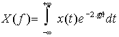
The important parameter in the sampling operation is the sampling rate which depends on the shape of the analog signal to be converted. In order to obtain the values that the sampling rate may take, it is necessary to carry out a spectral analysis of the sampled signal. First the concept of ideal sampling will be examined since the theory behind it is simple. In the case of ideal sampling it is assumed that the width of the sampling pulses is zero. Let x(t) be the signal to be sampled and x*(t) the sampled signal. The train of sampling pulses is represented by the function u(t). A signal x(t) is represented in the frequency domain by the function X(f) such that X(f) is the direct Fourier transform of x(t), that is :
The function X*(t) representing the sampled signal is given by:
x*(t) = x(t) u(t)
For ideal pulses of unit amplitude, period T and zero width, u(t) can be written as
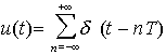
Where d (t) is the mathematical symbol used to represent an infinitely narrow pulse, the Dirac delta function, which is defined to have the following properties; d (t) = 0 for t ¹ 0,

The function x*(t) us then given by

In effect x (t) × d (t) = x (0) d (t) since d (t) = 0 for ¹ 0
Therefore the expression of the Fourier transform of the sampled signal which gives the spectrum of the signal is :

The spectrum of the sampled signal can be traced out using this last equation and generally it will be markedly different from the spectrum of the function x(t) corresponds a double infinity of lines of the same amplitude and of frequency
![]()
It can be anticipated intuitively that the substitution of the sampled function for the original function may only be made with great care, for we must be able to identify the original function again. It can be seen that the sampling operation can be realized if a relationship exists between the sampling frequency Fe and the maximum frequency Fmax of spectrum X(f). If the signal was sampled at a frequency Fe ³ 2Fmax the series of spectra will not overlap and it is then possible to separate the central band by means of an ideal low-pass filter. This relationship between Fe and Fmax is called the sampling theorem or Shannon's theorem. It may be stated thus; 'A signal x(t) whose spectrum is limited to the frequency Fmax is completely determined by the entire series of its samples taken at regular intervals T = (1/2Fmax).'
If this condition is not satisfied, the successive spectra partially overlap and it is no longer possible to recover the original information. In practice two restrictions have also to be taken into account; the upper limit of the spectrum of signal x(t) is not clearly defined and simply decreases above a given frequency, and an ideal filter does not exist so at the recovery stage a real filter must be used which will allow through some of the higher frequency bands. Therefore, in order to choose the sampling rate a knowledge of the shape of the spectrum of the analog signal is required and this reflects upon the speed of operation required of the converter.
In practice it is almost impossible to obtain ideal Dirac pulses and the pulses normally used always have a certain width t . The way in which this parameter modifies the spectrum of the sampled signal must now be examined. The first type of real sampling used is analog sampling; the pulses have a certain width t and signal x*(t) faithfully reproduces the signal x(t) for the duration of these pulses. The Fourier transform of the sampled signal can then be written:

Each repeated spectrum is multiplied by a constant factor(sinx)/x which depends on n only. Therefore the central part of the spectrum of X*(t) is not distorted. The overall width of the spectrum of such signal is reduced compared to that obtained using ideal sampling and it can be assumed to be limited to 2/t .
The second sampling method used is sample and hold. The pulse has a duration t and a constant amplitude. In this case the Fourier transform of the sampled signal is given by:

The error introduced when sampling a signal is an important problem since it affects the accuracy of analog to digital conversion processes. It is particularly significant when it is required to convert fast, discrete phenomena into digital form.
2.2. Recovery
Following a digital to analog conversion operation there arises the problem of recovery, for once the D/A operation is carried out the samples are reestablished and a function x*(t) is obtained whose spectrum is X*(f). The original signal x(t) which gave the train of samples must be reconstructed or recovered.
Let us consider a signal x(t) whose spectrum is limited to the frequency Fmax and which is sampled at a rate Fe - 2Fmax. It can be shown that x(t) can be expressed in terms of its samples as:
If a sample x (n/2Fmax) is selected and is fed through an ideal low-pass filter with cut-off frequency Fmax the response of the filter to such an input pulse will be;
![]()
The response of the filter to all the samples gives an output signal;
![]()
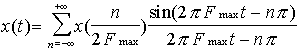
Ignoring the constant coefficient, this expression is identical to the original signal x(t). It is therefore possible to recover the original signal x(t) from samples taken at time intervals 1/2Fmax by passing them through an ideal low-pass filter having a cut-off frequency of Fmax. However in practice such a filter does not exist.
Nevertheless in order to recover the signal a classical low-pass filter may be used, for example a Butterworth or Tchebycheff type of filter which have the fidelity of the recovery will depend on the ratio Fc/Fe, Fc being the cut-off frequency of the filter, and on the sharpness or slope of that cut-off. The following expressions are for evaluating the error in recovery when a Butterworth filter is used. Consider a train of samples x*(t) which is passed through a filter having a transfer function H(f) (the transfer function of a system is the relation between the input and output signals of that system). The Fourier transform Y(f) of the output signal is given by
Y ( f ) = H ( f ) × X * ( f )
Another solution makes use of an interpolator. An interpolator is a device which allows the original curve to be reconstructed from the samples using linear segments. This operation always involves an error because of the approximation consists of holding the signal constant between two consecutive samples. This method is analogous to the hold device used in the 'sample and hold' method of sampling. This operation is called zero order interpolation or 'steeped' interpolation.
![]()
Its impulse response is a unit pulse of width T. The spectrum of the sampled signal is distorted since it is multiplied by the above function. The amplitude is multiplied by a function of (sin)/x and there is also a linear phase shift of -p f T. This distortion is significant even if the sampling theorem has been amply satisfied.
A more interesting solution makes use of linear interpolation; that is first order interpolation. The signal between time intervals nT and (n+1)T is a function of samples
x ( nT ) and x ( ( n - 1 ) T )
and can be expressed as
![]()
with
0 < q < T
k is positive and less than 1. When k is suitably chosen (of the order of 0.3 to 0.4) then a frequency response curve for the interpolator can be obtained which is almost flat within the band (0,1/2T) which is the useful band. However, as in the case of the zero order interpolation a certain phase shift will occur.
2.3. Quantization
Quantization is an operation that is met in systems used for transforming an analog quantity into digital information in the form of a message with a well defined length. Thus for a base b,n bits will allow N = bn distinct values to be encoded. It is possible to encode, that is to say recognize, only N well defined values of the analog quantity.
The quantization operation consists in replacing the exact value of the signal by one value taken from the N quantized values. Thus information consisting of a finite number of values is substituted for the possible infinite number of values of the analog quantity. Therefore it is essentially a nonlinear operation. In order to quantize a signal the amplitude axis is divided into levels which are assigned numbers. It is then only necessary to indicate the level number in which the tip of the vector representing the signal lies in order to define fully the amplitude of the signal. Therefore in order to carry out a quantization, the interval between levels must be defined. This interval is called the elementary level of quantization or quantum q. Any signal whose amplitude lie in the interval (nq, (n+1)q) will be described by the quantity nq.
2.4. Analog to Digital Converter
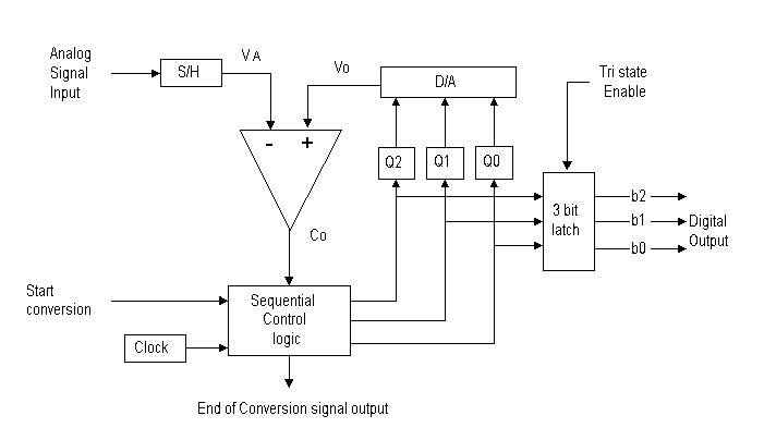
Figure 3: Block diagram of successive approximation A/D converter
There are many kinds of A/D converters, like parallel comparator (flash converter), successive approximation converter, dual slope converter, etc. Successive approximation converter has been chosen for this project. Figure 3 is the simple block diagram of successive approximation converter. It consist of a sample and hold circuit, a D/A converter, a operational amplifier, a sequential control circuit, a system clock and a 3 bit latch. It used 3 bits to illustrate the operation. Analog signal was inputted to the operational amplifier after the sample and hold process. The sequential circuit will generate different binary numbers to the D/A converter according to the input value of Co. The operational amplifier will compare the input of VA and Vo to generate the voltage of Co. This process will be repeated until the VA is closed to Vo. The 3 bits binary number will be latched to produce a output number of b0, b1, b2.
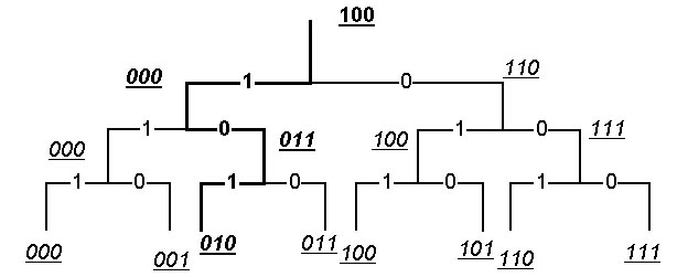
Figure 4
Figure 4 is an example to show how it works. For example, the input analog voltage VA is 1.8V. When the start conversion signal was received, the sequential control logic will set Q2 to 1, Q1 to 0 and Q0 to 0. The D/A converter will set Vo to 4V. Since Vo is greater than VA, Co will be set to 1 ( 1 represent high voltage level, 0 represent low voltage level ). Since Co input is 1, output to Q2 will be set to 0, otherwise if input is 0, Q2 and Q1 will be set to 1. Now Vo was changed to 0V since Q2,Q1,Q0 were changed to 000. The output of Co will be changed to 0 because VA is greater than Co. Since input Co was changed to 0. Output of Q1 and Q0 will be set to 1, otherwise if input is 1, Q0 will be set to 0. Vo will change to 3V, Co will be changed to 1 since Vo is greater than VA. Because input Co was changed to 1, Q0 will be set to 0, otherwise if Co is 0, Q0 will be set to 1. At this moment, Vo is set to 2V which is closed to input VA (1.8V). Q2,Q1,Q0 will be latched to form the output b0,b1,b2.
2.5. Digital to Analog Converter
Figure 5 is a simple block diagram of a digital to analog converter. It used 3 bit to illustrate the operation.
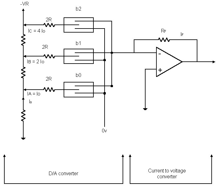
Figure 5 : Block diagram of digital to analog converter
b0,b1,b2 are the switches which represent the input values. If it switches to 1, the input voltage will be 1. If it switches to 0, the input voltage will be 0. IC is equal to 2IB and 4IA. Currents flow in b0 to b2 are different.
Since
Vo = IF RF
= ( IA + IB + IC ) RF
= ( b0 Io + b1 2Io + b2 4Io ) RF
= ( b0 + 2b1 + 4b2 ) Io RF
= ( b0 + 2b1 + 4b2 ) ( VR/8R ) RF
After we have understood the basic principle of analog to digital and digital to analog conversion, it needs to put theory into practice. This project is about to build a digital recorder which used to record the analog speech signal that was inputted from telephone system.
For instance, in an emergency telephone centre, usually the caller is in a emergency situation, phone may be cut off suddenly. A recorder is needed to record the conversation and replay the message immediately. Since most recorders are using magnetic tape as a media to record voice message, it takes time to rewind the tape before playback. Time is important in an emergency situation. A solid state digital recorder is a good solution. It can replay the message instantly after it has been recorded. It can always be put into record mode. We do not have to worry about the read write life time of the magnet tape. This recorder has the ability to record the previous 60 seconds speech message and can be stopped and replayed the previous 60 seconds message when required.
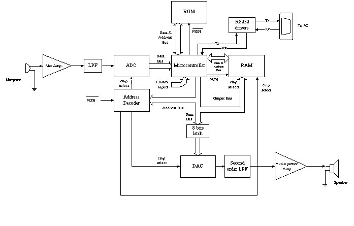
Figure 6 : System block diagram
Figure 6 is the system block diagram of the solid state digital recorder. To demonstrate the operation of this recorder, a microphone and microphone amplifier which has a low pass function have been added to the system. The analog telephone speech signal which to be recorded from the telephone system was already been filtered, so there is not necessary to have a low pass filter before the A/D converter. The one used here is just to stop the high frequency over 4kHz which was generated from the microphone amplifier.
Analog signal will be inputted to the successive approximation 8 bits output A/D converter. The sampled data will be stored into the RAM by the control of the microcontroller.
The control inputs are the input signals from the buttons of playback, record, and stop.
The PSEN is the output signal from the microcontroller which is used for the selection of RAM and ROM. If the PSEN is active low, ROM will be enabled, when it is active high, RAM will be enabled. The location of ADC and DAC are mapped in the location of RAM. RAM and the D/A or A/D converter can be selected individually by the selection from the address decoder.
The output analog signal from the D/A converter will be inputted to a audio amplifier.
Inside the D/A converter there is no latch function for the input data, so it is necessary to have a 8 bits latch for it.
The memory size of the RAM is 512k bytes. Since the microcontroller has only been able to address 64k bytes memory locations, so a special method for the address decoding of the RAM was adopted. 512k bytes RAM was divided into eight groups. Each group has 64k bytes. Five output pins from the microcontroller was used to select one of these groups. So 512k bytes of memory can be addressed under the software control.
In practice it is not possible to place this recorder near to the operator. Usually it is installed in a PABX (Public Automatic Branch Exchange) room. A remote control facility need to be adopted. The RS232 drivers are used to interface with a computer.
4.1. Sampling frequency
The stopband frequency Fmax of input signal from telephone system is 4kHz. The frequency of 3 dB down from the maximum amplitude is 3.4kHz. In order to make the series of spectra will not overlap and can be possible to separate the central band by means of an low-pass filter, The sampling frequency Fe must be greater than or equal to 2 Fmax ( Fe ³ Fmax ).

Figure 7 : Frequency spectrum
Figure 7 shows the frequency spectrum between the relationship of modulating frequency Fm and sampling frequency Fe. Fm is the frequency which is to be record. It is lain under the stopband frequency Fmax which is 4kHz. Fe is the sampling frequency, Fe-Fm and Fe+Fm are the frequencies which were generated with the present of Fe. To make sure Fe-Fm is not lower than the stopband frequency, Fe must greater than or equal to 2Fmax (8kHz) otherwise it can not be filtered by a low-pass filter. So 8kHz has been chosen for the sampling frequency in this recorder.
4.2. Memory mapping
Figure 8 is the memory mapping diagram. Inside the microcontroller, there are 256 bytes of Random Access Memory (RAM). 128 bytes are used for Special Function Register (SFR). 128 bytes are direct addressed which can be used for the stack or program usage.
The size of Read Only Memory (ROM) is 32k. Why used so large memory chip? Although the size of the executable binary file is just only 1214 bytes, it is because the address decoder for it is simple, it just needed to connect the address pin A15 to the chip enable pin of the ROM for the address decoding. The other reason is that it is difficult to find a small size of ROM, like 2716.
The D/A converter is at location FFFFhex. A/D converter is at FFFEhex. RAM is at 0000hex to FFF7hex. 8 bytes was lost for the selection of input and output device, so the size of the RAM was reduced to 8 x ( 64 x 1024 - 8 ) = 524,224 byte or 511.9k bytes.
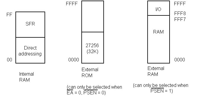
Figure 8: Memory mapping
The sampling frequency was chosen as 8kHz. A byte is used to represent the quantization level. There are 256 levels which is used to represent the analog voltage levels. In order to record 60 seconds of speech, 8,000 x 60 = 480,000 bytes are needed.
4.3. Address decoding
Figure 9: Address decoding
Figure 9 shows how each device can be selected. Each RAM chip has 128k bytes memory which was divided into two groups. Each group can be selected by the control of P1.4 which was connected to the address pin A16. P1.4 is the output pin from the microcontroller. P1.0 to P1.3 are the output pins from the microcontroller, one of the these pins can only be activated low by software control while the others are high.
The address decoder is used to generated the chip select signals for the address of each device.
Following are some descriptions for each part of the circuit. Mainly the circuit is divided into two parts, one is the analog and the other one is digital.
5.1. Analog
5.1.1. Analog to Digital Converter
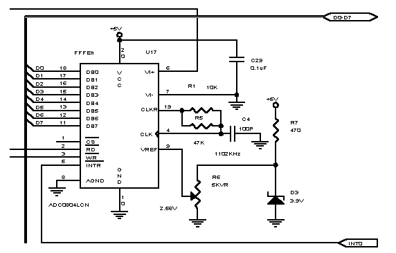
Figure 10 : Analog to digital converter
ADC0804LCN A/D converter has been chosen in the project. It is a CMOS 8-bit successive approximation A/D converter which use a differential potentiometric ladder similar to 256R products. This A/D appear like memory locations or I/O ports to the microprocessor and no interfacing logic is needed. A differential analog voltage input allows increasing the common-mode rejection and offsetting the analog zero input voltage value. In addition, the voltage reference input can be adjusted to allow encoding any smaller analog voltage span to the full 8 bits of resolution.
The analog input signal inputted to pin 6 is varied between 0V to 5V because of the supply voltage to the microphone amplifier is set to 5V. The VREF is set to 2.56V by adjust variable resistor R6. The supply voltage to R6 was regulated by a zenior diode D3. The conversion value for each LSB is equal to 2.56 x 2 / 256 = 0.02V. That means each quantization level is 0.02V.
To start the conversion a write signal must be inputted to the converter by set pin 3 to low state. It needs to take time for the conversion process. The conversion frequency can be calculated by use formula :
f = 1/ ( 1.1 x R x C)
f is the conversion frequency. The higher conversion frequency, the shorter conversion time is needed. The conversion frequency must within the range of 100kHz to 1460 kHz. According to the data book, if conversion frequency is 640 kHz, the conversion time will be 100 uS. In the circuit above, the R is equal to R1 + R5 = 8.2k. The C is equal to C4 = 100pF. So the conversion is equal 1102kHz.
After the conversion had been completed, pin 5 will change to low state. This is used to inform the CPU to read datum from it. After the datum have been read from the CPU, pin 5 will change to high again.
5.1.2. Digital to Analog Converter
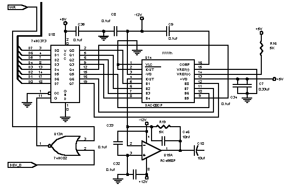
Figure 11 : Digital to analog converter
Figure 11 is the D/A converter circuit diagram. The DAC0800 is a monolithic 8-bit high speed current-output digital-to-analog converter (DAC) featuring typical setting times of 100ns. When used as a multiplying DAC, monotonic performance over a 40 to 1 reference current range is possible. The DAC0800 also features high compliance complementary current outputs to allow differential output voltages of 20 Vp-p with simple resistor loads. The reference-to-full-scale current matching of better than ± 1LSB eliminates the need for full-scale trims in most applications while the nonlinearities of better than ± 0.1% over temperature minimizes system error accumulations.
The noise immune inputs of the DAC0800 will accept TTL levels with the logic threshold pin, potential allow direct interface to all logic families. The performance and characteristics of the device are essentially unchanged over the full ± 4.5V to ± 18V power supply range; power dissipation is only 33mW with ± 5V supplies and is independent of the logic input states.
The RREF R16 = 5k, VREF = +5V. So, IREF = +5V / 5k = 1mA. When the input data are 11111111bin, the full scale output current IFS = IREF x 255 / 256 = 1mA x 255 / 256 = 0.996mA.
RF (R19) = 5k. The maximum output voltage = IFS x 5k = 4.98V.
So, the minimum output voltage change = 4.98V x [ 1/ ( 28 -1 )] = 19.53 mV.
That means when the input datum increase by 1LSB, the output voltage will increase by 19.53mV.
U18 is used to latch the input 8-bit data. Data will be latched only when in address FFFFh (DEV_0 = 0) and write cycle (WR = 0).
U15A is the current to voltage converter. C46 is used to filter the high frequency.
Since the stopband frequency w = 4kHz, the feedback resistor = 5kW .
So, C46 = 1/ ( 4 x 103 x 2p x 5 x 103 )
= 7.9nF » 10nF.
5.1.3. Lower Pass Filter

Figure 12 : Unity Gain Sallen and Key Second Order Low Pass Filter.
According to figure 7, a lot of unwanted signals was generated by the digital to analog conversion process. A low pass filter is needed to eliminate these signals. Figure 12 is a Chebychev low pass active filter. The stopband edge frequency fs is 4kHz. The passband edge frequency fp is 3.4kHz. The stopband loss of this filter can be up to -24 dB.
10nF was chosen as the value of capacitor C48. Resistor R43, R44 and capacitor C49 can be calculated by using the following equations.

5.1.4. Microphone amplifier

Figure 13 : Microphone amplifier
Figure 13 is a simple microphone amplifier circuit diagram. It provides better than 20-dB voltage gain.
C47 is used to form a low pass filter which to eliminate the unwanted high frequency. It provides -3dB gain at 4kHz.
Since
w = 4kHz and w o = 3.4kHz
Voltage gain at 4kHz =  = 0.64 » -3dB

R9 is used to provide a working current for the condenser microphone.
C5 is used to block the direct current between the R9 and input of the op-amp.
R10,R12,R16,R18 provide the bias voltage for the op-amp.
5.1.5. Audio Power Amplifier

Figure 14 : Audio power amplifier
Figure 14 is a one watt audio power amplifier. The power gain is set to 20 by disconnected pin 1 and 8. R22 and C14 are used to form a high pass filter which shunt the high frequency to ground. The power gain can be increased up to 200 by connect a 20uF capacitor between pin 1 and pin 8. LM386 can be operated within the supply voltage 4 volt to 12 volt. The quiescent current is just only 4 mA. It is ideal for battery operation.
5.2. Digital
5.2.1. Microcontroller
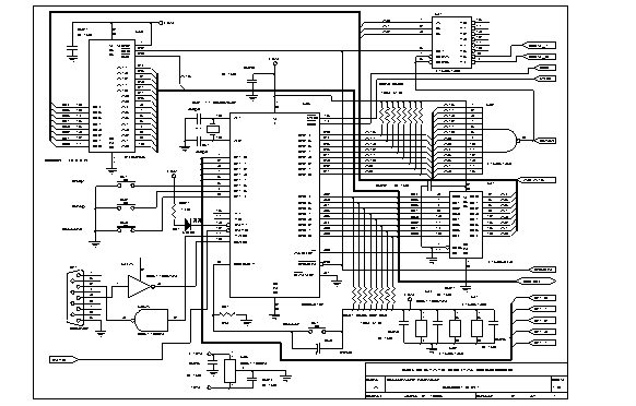
Figure 15
Figure 15 is the circuit diagram of the microcontroller and the peripheral circuits. U5 80C31 is a 8-bit microcontroller. It has four input and output ports. Two of them had been used for the data bus and address bus by connected pin 31 to ground. When instruction was fetched from the ROM, pin29 (PSEN) will be changed to low state, if data is fetched from RAM or I/O port, it will be in high state.
U1 is used to latch the address pin from A0 to A7 from the combined address and data port P0. U2 and U4 form a address decoder for address FFFFhex and FFFEhex. S4,R4 and C3 is the reset circuit. C3 is used when this microcontroller is switched on. S4 is used for to reset the circuit when required.
D4 is the status LED. When it is on, it shows that message had been recorded, it is ready for playback by press the play button. When it is off, it shows the record is in idle mode or stop mode. The recorder is in record mode when the LED was flashing quickly or in playback mode when it was flashing slowly.
U3 is the Read Only Memory (ROM). ROM was mapped into the lower 32k bytes by connected A15 to chip enable pin. P1.5 to P1.7 was configured as input ports for the play, stop and record buttons. There are no pull up resistors for these buttons. because a byte will be written to P1.5 to P1.7 once the program have been started to make them in the high level state. U6A and U7A are the RS232 drivers for communication with PC. P1.0 to P1.4 are the output pins which are used to enable the RAMs.
5.2.2. Random Access Memory (RAM)
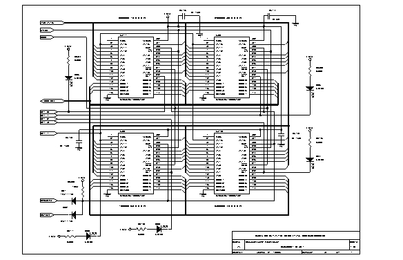
Figure 16
Figure 16 is the circuit diagram of the RAM bank. Each of chip contain 128k bytes of memory. Totally there are 512k bytes. P1.0 to P1.3 control pins from the microcontroller are used to select one of these four RAMs. P1.4 is used to select the upper 64k or lower 64k bytes memory. LED D5 D8 are used to show which RAM chip has been selected. LED D9 shows the lower 64k or upper 64k bytes memory have been selected. D1 and D2 and R39 form the a wired AND circuit. Because just only one 'AND' logic gate has been used, it is better to use a wired logic instead of to choose a 7408 TTL integrated circuit.
6.1. Address pointer
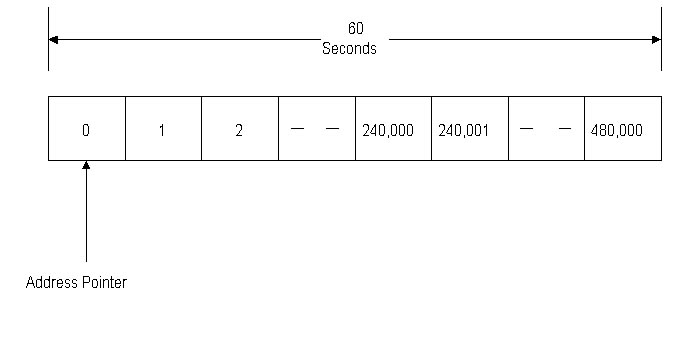
Figure 17
Figure 17 shows the allocation of each byte of memory in the Random Access Memory. Since simpling frequency is 8kHz and a byte is used to represent the quantization level, total number of bytes for the memory to store 60 seconds of speech is 480,000 ( 8,000 x 60 ) bytes.
There is a pointer used to point to the address of each byte. Data will be stored to the address which the pointer is pointing at. The pointer will be increased by one after a byte was stored to the memory. When the record button is pressed, the pointer will be started at the location of the first byte. The pointer will be reset to the location of the first byte after a datum was stored to this location. It is like a loop counter.
The pointer will stop to increase when the stop button was pressed. Pointer will be reset to zero (the location of the first byte) when the recorded time is less than 60 seconds. After the play button was pressed data will be fetched started from the first byte and stop at the location where when the stop button was pressed. If the record time is exceeded 60 seconds address pointer will not reset to zero and it will be stopped at the location where when the stop button was pressed. Data will be fetched started from the location just one byte after the one where the pointer is pointing at and stop at the location where the stop button was pressed. e.g. If the record time is exceeded 60 seconds, the address pointer will stop at the location of byte 240,000 where when the stop button was pressed. After the play button was pressed data will be started to fetch from the byte 240,001 and will stop at byte 240,000 (address pointer will be reset to 0 after it reach byte 480,000). The program has been able to check the record time whether it is more than or less than 60 seconds, in order to take the appropriate action.
6.2. Program flow
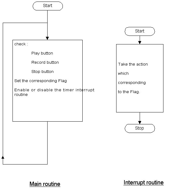
Figure 18
Figure 18 is a simple program flow diagram. Mainly it is divided into two parts. One is the main routine and the other is the timer interrupt routine.
The task of the main routine is to check the commands which inputted from the three buttons or the serial communication port (RS232) and to set the corresponding flags. e.g. Record flag will be set when record connand was inputted. The timer interrupt routine will be enabled after the play flag or record flag has been set. If the stop command is inputted, play flag and record flag will be cleared and the timer interrupt routine will be disabled.
Timer interrupt routine can be seemed as a subroutine, it will activated in every fixed time interval. The main routine will be stopped when the interrupt routine has been activated. The return address will be saved automatically and the registers which will be affected by the interrupt routine also have been saved. The main program will be resumed after the timer interrupt routin was ended. The task of the interrupt routine is to check the play flag or record flag. When record flag was set, datum will be taken from the A/D converter and stored to the RAM. When play flag was set, datum will be taken from the RAM and output to the D/A converter. Figure 19 and 20 are the detailed flow diagram for the main routine and timer interrupt routine representatively.
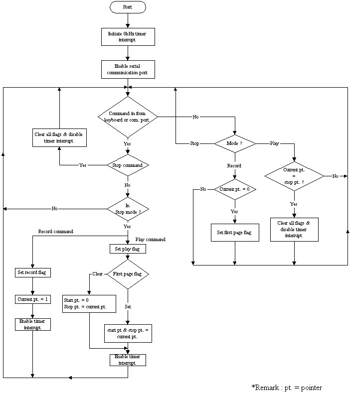
Figure 19
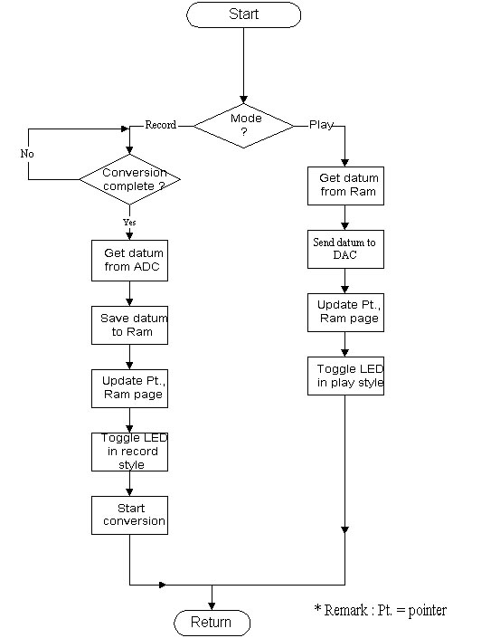
Figure 20
There are some problems were arisen after the board had been built.
7.1. Noise
Noise is the most serious problem that was encountered. A high frequency signal was mixed with speech signal together appeared on the speaker. By examined the frequency spectrum of the playback signal. There are some unwanted signals which is the harmonic of the sampling frequency. Since the sampling frequency fs mixed with the modulating freuency fm, fs-fm and fs+fm will be generated. Also the present of the harmonic of fs fs-fm and fx + fm influence the main modulating frequency fm.
A high attenuation stopband loss filter was introduced to solve this problem. It is a unity gain sallen and key second order low pass filter. It was placed behind the D/A converter.
By testing with this filter a set of data are shown below :
Frequency |
Input voltage (p-p) |
Output voltage (p-p) |
100Hz |
11V |
11V |
158Hz |
11V |
11V |
251Hz |
11V |
10.2V |
398Hz |
11V |
10.0V |
631Hz |
11V |
9.4V |
1Kz |
11V |
6.8V |
1.584KHz |
11V |
3.9V |
2.511KHz |
11V |
1.6V |
3.329KHz |
11V |
8V |
4.121KHz |
11V |
1.1V |
6.3KHz |
11V |
0.8V |
10KHz |
11V |
0.1V |
15.8KHz |
11V |
0.04V |
25.118KHz |
11V |
0.015V |
39.810KHz |
11V |
0.0075V |
50.118KHz |
11V |
0.005V |
Table 1

Figure 21
From figure 21, voltage at frequency 3.4KHz is 8 V, 1.1V at 4kHz. The attenuation is over -20 dB at frequency 4KHz. The noise was improved a lot after the filter had been added.
Although the noise generated by the sampling frequency 8KHz had been depressed. There are still some noises which influence the speaker even not in replay mode. These noises are came from the digital circuits. Since during the switch on and switch off process, a serious interference was generated. These noises influence the power supply as well as the audio power amplifier. To eliminate these noise, a small capacitor 0.1uF was placed between the voltage supply input pin and the ground for all TTL integrated circuit.
7.2. Audio level
It will has a better playback quality if the speaker is closed to the microphone. But distortion had been occured when the sound level was too high.
The microphone amplifier was introduced only for the demonstration purpose. If this amplifier has been used permanently. A Automatic Gain Control (AGC) circuit is better to introduced.
7.3. Improvement
Due the time limitation, some further improvement had not been done. They are data compression and data transmittion.
7.3.1. Data compression
To examine the data which were stored in the RAM bank a subroutine program had been added to the main program temporarily to fetch data from the RAM bank and transmitt to the computer through the RS232 port at the time when a download command was received. Follwing is the source code of this subroutine :
DOWNLOAD:
JB RECORD_MODE,DOWNLOAD_EXIT
JB PLAY_MODE,DOWNLOAD_EXIT
JNB RX_FLAG,DOWNLOAD_EXIT
MOV A,COMMAND
CJNE A,#44H,DOWNLOAD_EXIT
;DO THE DOWNLOAD
MOV R0,#0
MOV R1,#0
DELAY_AGAIN_1:
MOV R0,#0
DELAY_AGAIN_2:
INC R0
CALL DELAY
CJNE R0,#0,DELAY_AGAIN_2
INC R1
CJNE R1,#10,DELAY_AGAIN_1
CLR RX_FLAG
MOV DPTR,#0
DOWNLOAD_AGAIN:
CALL CHECK_RESET
CALL CHECK_KEY
JNB RX_FLAG,DOWNLOAD_PASS
MOV A,COMMAND
CJNE A,#53H,DOWNLOAD_PASS
JMP AGAIN
DOWNLOAD_PASS:
CLR RX_FLAG
MOVX A,@DPTR
MOV R0,A
MOV R1,A
; R0 IS D7 - D4
ANL A,#0FH
ORL A,#30H
MOV R0,A
; R1 IS D3 - D0
MOV A,R1
SWAP A
ANL A,#0FH
ORL A,#30H
MOV R1,A
;R1 IS D7 - D4
CLR ES
MOV SBUF,R1
JNB TI,$
CLR TI
; R0 IS D3 - D0
MOV SBUF,R0
JNB TI,$
CLR TI
INC R3
CJNE R3,#26,PASS
MOV R3,#0
MOV SBUF,#0DH
JNB TI,$
CLR TI
MOV SBUF,#0AH
JNB TI,$
CLR TI
JMP PASS_1
PASS:
MOV SBUF,#20H
JNB TI,$
CLR TI
PASS_1:
SETB ES
INC DPTR
MOV A,DPH
CJNE A,#7FH,EXIT_
MOV A,DPL
CJNE A,#FFH,EXIT_
DOWNLOAD_EXIT:
RET
Following are part of the data which were taken from the RAM bank :
00 7> 7< 7= 7< 7; 78 7: 79 79 7< 7> 7< 7; 7: 7: 7; 79 7: 79 7< 7; 7: 7: 7; 7<
7< 7? 82 85 82 86 87 8= 8: 86 82 7< 7= 78 79 7: 7: 78 7; 7? 84 87 86 84 81 80
7< 7< 7= 7; 78 77 77 7: 7; 7< 7: 7= 7< 79 79 7: 7; 7< 7; 7: 7> 7< 79 79 7= 7?
81 81 83 87 8; 8; 88 8; 84 80 7< 79 79 79 75 77 7; 7? 80 85 87 88 83 81 7> 80
7> 78 77 77 77 77 77 7: 7> 7= 7: 79 7= 7; 79 79 7; 7= 7< 79 7: 7? 80 7? 7? 83
85 86 87 8= 8< 8: 80 7< 7> 80 78 77 76 79 7: 7< 7? 87 8: 84 83 82 84 80 7< 7:
7: 78 74 73 79 7< 7< 7: 7: 7< 7; 79 7: 7= 7> 7; 78 7; 7< 7< 7< 7= 7? 84 81 83
87 8= 8? 8< 87 84 80 7< 7: 79 7; 78 78 78 78 83 84 84 85 86 84 80 7> 7> 7> 7:
75 75 75 75 75 77 7: 7; 78 77 7: 7; 7? 7? 7? 7> 7< 79 79 7; 7= 80 7? 7? 83 87
8: 8? 8? 8= 89 82 7< 7; 7; 7: 79 77 78 7; 7> 82 86 88 87 84 80 7> 7? 80 7< 78
76 75 72 73 75 77 79 79 78 7: 7= 7? 7? 7= 7> 7> 7: 78 79 7; 7= 7= 7= 7? 85 86
87 87 8= 8? 8< 88 85 81 80 7= 7: 7< 7; 7: 7; 7< 7? 85 84 83 82 80 7? 7= 7> 7=
7: 78 74 74 73 75 77 79 7: 7: 79 79 7; 7< 7< 7= 7: 79 76 79 7; 7> 7? 81 80 81
81 82 85 86 8: 89 88 88 88 88 85 83 81 7> 7< 7< 7; 7= 7? 80 80 80 80 7= 7= 7=
We found that some of data were appeared continuously. Data compression technique should be introduced to save memory space.
Here is a method to compress the data :
We can use two bytes to represent a series of duplicated numbers. The first byte can be used to represent the value of the data, the second byte represent the number of times that they were appreared. We can choose a byte to inform the entry of data compression procedure. The best choice is hexadecimal value FF or 00.
To compress the data, the microcontroller will write a value of 'FF' to the memory when 3 bytes of data appear to be the same, and then it will wait for the end of the appearance for these duplicated number. When a byte of data appeared to be different from the previous one, microcontroller will write the value of the duplicated number to the memory and the times that they had been appeared and finished the data compression procedure.
During replaying the stored message, when a byte of hexadecimal value FF was taken from the memory, the microcontroller will know that the two bytes of data following are the data that had been compressed.
Following is the flow diagram of the data compression procedure.
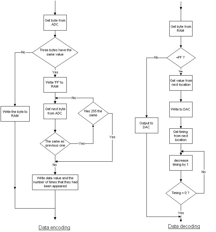
Figure 22
Since the sampling frequency is 8Khz, that means a byte of datum will be stored in every 125uS. The clock frequency for the microcontroller is 11.0592 MHz. Each machine cycle needs 12 clock cycle. 43 machine cycles had already been used in the timer interrupt routine for record and 41 clock cycles for playback. That means almost 45uS had been used. In the main program, it needs to take time to update all the pointers and control the selection of RAMs. There has not enough time for it to do the data compression.
Although we may change a faster operating speed microcontroller, but we have to change all the program. It seems not possible to do that. The another possible way is to add a new same type microcontroller which is just used to take the data compression task. It receives the data from the main microcontroller and do the data compression. After the data have been compressed, send the data to the RAM bank. But due to the time limitation, this method had not been implemented.
7.3.2. Data transmission
It is a good idea to send the sampled data to a computer and save it as a file. File can be send back to the recorder if required. We can use the RS232 communication link for this purpose. But RS232 is a serial communication link. If send 512k byte of data in a 9600 bit per second, it will take 550 seconds or 9 minutes to complete the transmition. This method seems not possible. The possible way is to send the data in parallel. A parallel port need to be introduced. Use this port to connect to the Centronic communication port (parallel port) which usually attached to a PC for the data transmittion.
The aim of this project is to convert analog speech to digital form and store the previous sixty seconds of sampled form. Finally, this task can be achieved.
Due to the time limitation there are still some improvements which have not been done. Like to implement the data compression, download the data from the RAM bank to PC, change the PC control program so that it can save the data into a file format.
9. Bibliography
1. BERNARD LORIFERNE : "Analog-Digital and Digital-Analog conversion",WileyHeyden Ltd.,1983
2. Buchsbaum & Gina Weissenberg, M.E.E. : "Microprocessor & Microcomputer Data Digest", Prentice-Hall Company,1983.
3. CLAYTON : "Data Converters", Department of Physics, Liverpool Polytechnic,1982.
4. GILBERT HELD & Thomas R. Marshall : "Data Compression", John Wiley & Sons Ltd., 1991.
5. John Clark Craig : "Visual Basic Workshop", Microsoft Press, 1993
6. R.M.MARSTON : "OP-AMP & OTA Circuit Manual",Butterworth-Heinemann Ltd. 1993
7. RH DADD : "Microcontroller note 2 RHD8051", University of Portsmouth, 1995.
8. Richard Mansfield : "The Visual Guide to Visual Basic for Applications", Ventana Press, 1994.
9. RUDOLF F. GRAF : "The Modern Amplifier Circuit Encyclopedia", TAB Books,1992
10. Steve Dolan : "INSTANT Visual Basic 3", Wrox Press Ltd.,1995