A
Personal Network Analyzer Built With Only 15 IC's
 By: Steve Hageman
This article originally appeared in the January and February 1998
issues of QST. It is reprinted here courtesy of the ARRL and
QST.
Originally copyrighted QST 1998, all rights reserved.
NOTE: You may wish to download the schematics and parts lists for
this article here. For other project questions please visit the
PNA FAQ page.
My first network
analyzer was designed around 1985. It used a general purpose analog
VCO (an Intersil ICL8038) as the driving source and a pair of IC
RMS-DC converter chips as receivers. I can remember the date because
I programmed it through some A/D and D/A converters from my Apple II
computer. It had it's limitations, the dynamic range was only about
30 dB and the frequency topped out at 100 kHz. Good enough for audio,
but not even close for the simplest 455 kHz IF.
This design started
out a few years ago when Numerically Controlled Oscillators (NCO's
also are called Direct Digital Synthesis or DDS chips) started
appearing in designs [1] based on the Harris Semiconductor HSP45102
DDS Chip. This part allowed a two chip solution to generating sine
waves from 0.01 Hz to around 16 MHz with 32 bits of digital
programming. Wow, to build a low noise PLL to do this would involve
lot's of bench debugging time, and be slow to change frequencies
because of the low frequencies involved.
In 1994 I built my
first of several DDS oscillators based on the Harris chip. When they
are clocked at 40 MHz, 10 Hz to 10 MHz programming is very clean and
reasonably spur free. The output can be coaxed to 16 MHz output, but
Nyquist sampling limitations and aliased spurs start to be only -20
dBc down from the main carrier. For more information on DDS methods
and limitations see the references at the end of this article.
Late in 1996, while
working on a 60 kHz, WWVB receiver I was experimenting with a
Philips, NE604A IC. This part is essentially a 80 dB LOG FM IF strip.
I was using it because a feature of the chip is it's Received Signal
Strength Indicator or RSSI output. The RSSI output gives a fairly
accurate voltage that is proportional to the input IF voltage over a
-20 to -100 dB range, that's 80 dB or so of dynamic range from a
single low cost IC. While experimenting with the part I found that
while it was designed for narrow bandwidth 455 kHz or 10.7 MHz IF
applications it would work with a dynamic range of 60 dB or so in a
wide band mode.
The connection was
made, using a Harris based DDS chip and the NE604A I could now build
a network analyzer that had 50 dB of dynamic range and a frequency
range up to 16 MHz. This would be suitable for nearly all of my IF
work and plenty of dynamic range would allow accurate measurements of
high loss filters and high gain amplifiers. So this design was
born.
Basics Of A
Network Analyzer
A basic network
analyzer is designed to show graphically, a plot of the voltage gain
or loss of a network versus frequency. These sorts of plots are
called Bode plots and are frequently shown in textbooks on circuit
design and are produced by computer circuit analysis programs. A
network analyzer consists of a swept frequency source that drives the
network under test and two receivers. The first receiver is used to
accurately measure the Reflection or input voltage to the network.
The second receiver is called the Transmission channel and is used to
measure the output of the network under test. The ratio of the output
to the input level is displayed as dB and is the voltage gain or loss
of the network. The source is swept over the frequency range of
interest and a Bode response plot of the network results.
Commercial network
analyzers range in cost from several thousand dollars on up and may
be able to analyze circuits in the frequency range of milli hertz to
microwave frequencies of 50 to 100 GHz. There are many special
designs available that allow fast sweeps for automatic testing or
very wide dynamic range for highly precise measurements.
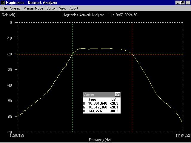 Example
plot of the PNA being used to measure a 10.7 MHz ceramic IF
filter.
Example
plot of the PNA being used to measure a 10.7 MHz ceramic IF
filter.
The Personal
Network Analyzer
The circuit presented
here deviates from most commercial network analyzers in that the
inputs are broadband. Commercial analyzers use very narrowband
receiver inputs and at higher frequencies use superhetrodyne down
conversion to convert the response at a lower frequency. The tradeoff
of using wideband inputs makes the receivers respond the sum of all
voltages input over the full bandwidth of the receiver. This lowers
the dynamic range of the design and it also decreases the achievable
accuracy. These tradeoffs were made because it lowers the parts count
and total complexity of the design by at least 50%.
The personal network
analyzer shown in figure 1 has the same basic blocks as a commercial
analyzer. It has a swept source frequency, and two receivers. One
receiver for the reflection signal and one for the transmission
signal. The ratio of the transmission to the reflection signal is the
response of the network under test. To program the analyzer and
display the results, an RS232 communications link is used. This
allows a program running on a PC to set the frequency, read the
receiver inputs and plot the results directly on the PC's
screen.
Receiver
Circuit
The Reflection and
Transmission receivers are identical in design and are based on the
Philips NE604A IC. As shown in figure 2, the NE604A is used as a high
dynamic range, wideband RMS to DC converter. The RMS voltage at the
input of the IC is converted to a linear DC voltage at it's output by
a series of limiting amplifiers. The limiting amplifier action serves
to convert a 10 times change in input signal to a linear output
voltage or about 44 mV output per dB change on the input (at pin 5 on
the NE604A). Used by itself the NE604 responds to signals in the
microvolt range to about 0.32 volts peak to peak.
To extend the dynamic
range and increase the input impedance to the receiver, a buffer
amplifier consisting of an Analog Devices AD847 is used ahead of the
NE604A. A 10 K ohm resistor is used at the input of the buffer to set
the input impedance of the receiver at 10 k Ohms, the AD847 buffers
the input voltage to drive the lower impedance of the NE604A.
The AD847 is followed
with a switchable 30 dB attenuator. The attenuator was chosen to be
about 1/2 the available dynamic range of the receiver alone, thus
extending the total system dynamic range significantly. The
attenuator is controlled by the PC program operating the analyzer
automatically to maximize the dynamic range of the receiver. With the
attenuator switched in the NE604A does not overload with signals up
to 10 volts peak to peak.
The AD847 was chosen
because it has a wide bandwidth of 50 MHz and it's very low noise.
The low noise is significant because it helps to keep the total noise
floor down in this wideband design.
The RSSI output of
the NE604A (pin 5) is buffered and filtered by a low frequency LM741
amplifier. The RSSI voltage is then sent to the microprocessor board
for A/D conversion.
The one adjustment in
this entire design is the gain adjust on the RSSI output voltage.
Since the dynamic range of the NE604A is in excess of 80 dB in narrow
band applications the RSSI voltage can swing from 0.2 volts to 4.8
volts. In this wideband design the noise floor is quite a bit higher
(only about -60 dB). This makes the RSSI voltage range from about 1.5
to 4.8 volts.
The A/D converter
used (on the microprocessor board) has an 8 bit, 0 to 5 volt input
and if the RSSI voltage swings from 1.5 to 4.8 volts a reduced
dynamic range is available. To make full use of the A/D converters
input range, the RSSI voltage is offset negative by about 1.5 volts
by the gain trimpot and resistive divider. This makes the RSSI range
from about 0 to 3.3 volts. The 741 OPAMP is set for a gain of 1.5 to
provide the A/D converter with a full 0 to 5 volt input swing.
The gain adjustment
is used to set the full scale voltage on each receiver to be the
same, thus allowing maximum dynamic range to be achieved. The
ultimate resolution of the design is then approximately, 60 dB / 256
possible output codes of the A/D converter or about 0.23 dB per A/D
converter LSB (Least Significant Bit) change.
DDS Source
Circuit
The basic circuit of
the DDS source built around the Harris Semiconductor HSP45102 has
been around for several years [1]. This circuit is upgraded from the
others in that I have added AC Coupling to the output along with
three programmable outputs and a 16 MHz active low pass filter to
control the harmonics some and flatten the frequency response.
The attenuators
provide computer controlled outputs of 5, 2.8, 0.3 and 0.032 volts
peak to peak. Having the source output switchable also helps increase
the dynamic range of the analyzer by allowing the control program to
reduce or increase the input voltage to the network under test to
keep the receiver inputs in the active portion of their range. The
attenuators are achieved by using simple shunt resistors to divide
the approximately 160 ohm output impedance of the DAC to a lower
voltage swing.
Controlling the
sources absolute amplitude accuracy is not required in this design
because the receivers operate ratiometrically. That is the ratio of
the input to output is important, not the absolute value of the input
voltage or output voltage.
The output of a
digitally sampled sine wave has what is called a "Sine X over X"
response. What this means is that as the output frequency approaches
the clocked or sampled frequency the voltage rolls off in a sort of
sine wave shaped response. The first null of the roll off is at the
clock frequency. The low pass filter was optimized with the RF
computer analysis program Touchstone [2] to provide slight peaking at
the cuttoff frequency to compensate for the roll off. The resulting
response is flat to within 1 dB from 10 Hz to 10 MHz and falls off to
about -3 dB at 16 MHz.
The HSP45102 is a
single chip circuit that when programmed with a 32 bit serial word
will produce a digital equivalent of a sine wave on it's output. The
output frequency is changeable by sending another 32 bit word to the
device. The high speed version of the IC allows clocking at 40 MHz.
Although the device operates with a 12 bit internal word size and has
the capability to drive a 12 bit DAC, I have used (like all the
others) the Harris CA3338. The reason is simple, this is a readily
available, relatively low cost IC and it is capable of being clocked
at 40 MHz also. 12 bit DAC's capable of operation at these
frequencies will do a great job of lightening your wallet and the
performance delta from going from 8 to 12 bits is not great enough to
warrant the extra cost.
The DDS circuits that
I have built have harmonics and spurs below -50 dBc up to 5 MHz and
degrade to -40 dBc at 10 MHz. Above 10 MHz the alaising spurs come up
to the -20 dBc level and start to appear below the programmed
frequency. For example at 16 MHz output frequency, the largest
aliased spur is actually around 5 MHz.
The master clock for
the DDS is provided from a 40 MHz, CMOS oscillator. These "Canned"
oscillators are very low cost and typically accurate to well within
0.01%. The clock is what sets the absolute accuracy of the output
frequency. By using a 0.01% oscillator the output frequency will be
within +/-1000 Hz when programmed at 10 MHz.
Microprocessor
Circuit
The control
microprocessor is the very popular PIC series from Microchip
Technology (Chandler, AZ). It was chosen because it is a truly
"Single Chip" computer and it's very low development and support
cost. I built a complete development system including a programmer,
first rate C Compiler [10] and UV Eraser for under $200.00.
The parts are readily
available and when the reprogrammable types are used they can be
erased and used over again in other projects.
One of the selling
points of the 16C71 device used is that it is very easy to program
the device for RS232 serial communication using only 3 wires to the
host PC. The 16C71 also contains a four channel, 8 bit internal A/D
converter.
The basic operation
of the uP is to read commands from the RS232 port and set the source
frequency, source and receiver attenuators and read the receiver
output voltages (Via the PIC's built in A/D converter). A small C
program was written to interpret ASCII commands from the RS232 line
and set the appropriate bits high or low on the PIC's output pins.
Full software handshaking is implemented by sending back an
acknowledgment character ('*') after each successfully read command.
If the synchronization between the PC and the PIC is broken for any
reason the PC can then sense the error and resynchronize the
programs.
When operating at 4
MHz the power dissipation is just a few milliamps and the RS232
connection can operate comfortably at a standard 9600 baud.
The internal, 4
channel A/D converter of the 16C71 device makes it easy to get data
from the real world and send it along the RS232 into the PC for
processing.
The availability of
low cost, efficient C [10] and Basic compilers [11] for these devices
also means that you don't need to learn yet another assembly language
to put these processors to work. You can work in a comfortable high
level language instead.
Of course these
functions could have been implemented with half a dozen discrete
logic chips and the result would have been the same. But the design
and building time was cut from a week to just an afternoon using the
PIC microprocessor.
Power Supply
Circuit
The power supply is
so straight forward that it doesn't hardly even need mentioning. A 25
volt center tapped transformer (available from Radio Shack) is used
to provide unregulated +/- 17 volts to the three terminal regulators.
The only thing of
special note here is that the regulator used for the +5 volt output
should be the fairly accurate (+/-2% or better) type specified. This
is because the regulator is used to power the microprocessor and the
microprocessor uses this voltage as a reference for it's internal A/D
converter. It is desirable to keep this voltage as close to 5 volts
as possible to keep the dynamic range of the receivers
optimized.
The +5 volt regulator
should be mounted to a small heat sink as it dissipates some power
due to the +17 volts at it's input.
Building The
Network Analyzer
Most of the circuits
are noncritical and can be built in just about any way you want. I
built all of my circuits "Breadboard" style on small pieces of copper
clad PCB. The copper clad provides a convenient ground plane and the
circuits are built 3-Dimensionally above the board.
I built the source
and receiver circuits on small pieces of copper clad that fit in
small aluminum boxes of the type that Radio Shack sells. The small
enclosures fully enclose the operating circuits and further help to
reduce the noise floor.
The receiver circuits
need some special care when building however. Separation from the
input to the receiver to the input of the NE604 is a must if you are
going to achieve the 60 dB dynamic range possible with this design.
Because of the high impedance levels here (the NE604 has a 1.6 k
input impedance) capacitive coupling is the mechanism that we need to
protect from. I built my receivers pretty much like the schematic
shows with the input circuit on top then the input signal folding
back past the NE604 to the NE604's input. This created a coupling
path from the middle section of the NE604 amplifier chain to the
input. The net effect is regeneration, if not downright oscillation.
The noticeable effect of regeneration is a noise floor only 30 or 40
dB down from full scale. To cure this problem I fashioned some
shields from copper foil wrapped in insulating tape and placed them
as shown on the schematic. The noise floor should drop considerably
as they are positioned correctly in the circuit.
The DDS source
circuit has just the opposite problem however. Because the impedance
levels here are below 300 ohms, the coupling mechanism is magnetic.
This means that circuit stray inductance is important. To keep the
inductance to a minimum the wiring loop areas must be kept to the
absolute minimum. This is achieved by keeping all lead lengths as
short as possible and making short connections to the ground plane.
Because of the high
speeds and large digital switching current on this board, decouple
everything! The DDS chip needs to be decoupled to prevent ringing
that will feedthrough to the DAC. The DAC needs to be decoupled to
prevent digital noise from appearing at the output of the DAC.
The grounds from the
DAC to the output active filter must also be as direct as possible.
Otherwise any ground "Bounce" due to currents flowing through ground
inductance will just show up directly at the output of the
filter.
Each of the circuits
ground plane's were tied to the shielding box with a piece of braid
that is soldered to the copper clad ground plane and just slips
between the box halves when assembled. The boxes themselves were then
grounded together with more braid.
The PC Control
Program
The PC control
program called "Analyzer.EXE" is where the hardware gets all it's
instruction as to how to perform. The basic sequence is as
follows,
1) Setup
for a sweep, get start and stop frequencies and number of points to
be swept.
2) Get any other
information about hardware external conditions that the hardware
can't determine on it's own (i.e. is a X10 probe connected to an
input?). Also set the min and max source amplitude limits if
needed.
3) Start the
sweep,
a) Send a
frequency word to the source.
b) Autoscale source
and receiver attenuators to keep the dynamic range optimized (if
needed).
c) Make the receiver
readings. Repeat if not settled.
d) Repeat for all
frequencies in the sweep
4) Plot the sweep
data (i.e. Make a Bode Plot).
5) Allow the user to
view, measure with cursors, zoom around and print the resulting Bode
Plot at his PC.
A continuously
updating, single frequency "Manual Mode" is also available which
allows peaking, nulling or tuning of the network under test in real
time.
The program was
written in 16 bit, Visual Basic for Windows and will run under
Windows 3.1 and Windows '95. Visual Basic is perhaps the easiest way
to program under Windows yet devised and allows easy graphics
programming which is a large part of this program.
The program was
written in three basic modules, the first is the low level hardware
control. This is where the code actually communicates to the hardware
via the RS232 to do such things as: Set the DDS frequency, make an
A/D reading or switch an attenuator in or out.
The next layer is the
high level hardware control where actual frequency sweep takes place
and the autoscaling of the hardware attenuators takes place. The
result of this layer is a data array of frequencies and dB ratio
values for later display.
The last layer is the
graphics display, the functions here control how the data is
displayed, allow zooming in on the data and manipulate the on screen
cursors.
Using a PC as a
controller has the advantage of nearly unlimited number crunching
ability. This comes in very handy when we want to convert nonlinear
or slightly nonlinear functions to linear ones for display. The
nonlinear function I'm referring to here is the RSSI output of the
NE604 chip. The measured linearity over a 60 dB range is shown in
figure 6, the bumps in the curve are about +/1.5 dB peak to peak.
Just because the chip
has some nonlinearities doesn't mean that we have to live with them
however. Using a precision set of attenuators I found the actual RSSI
output for a known input over an 80 dB range of operation in 5 dB
steps. I then wrote a function in the program that uses the measured
data and linearity interpolates between points to improve the
linearity to less than 0.4 dB.
As for speed the
program is pretty much limited by the RS232 transmission time. On any
computer faster than a 386, 33 MHz the RS232 time and not the
computer speed will be the limiting factor. On my development system
(a 50 MHz, 486) the program can do slightly better than 100 frequency
points per minute.
Adjustments /
Performance Checks
The only adjustment
to be made on the analyzer is to adjust the RSSI full scale output.
This is most conveniently done by using the PC control program in the
"Manual Mode" and connecting the receiver inputs to the source output
(use a 50 ohm termination on the source output). Set the source for a
-20 dBv at 100 kHz output. Set the receiver attenuators to off. Then
adjust the gain control (through the receiver shielding box) to be
exactly 230 A/D counts on both receiver channels.
After this is done
remove the cover from both receiver channels and measure the voltage
at the bottom end of the 100 k ohm RSSI resistor. This voltage should
be around -1.5 volts and the same for both channels. If it is much
more negative then this suggests that the noise floor is too high.
High noise floor is almost always caused by improper shielding around
the NE604. Work on the shielding and make the gain adjustment again
until the desired results are achieved.
Where do we go
from here?
The usefulness and
circuit insight gained by actually measuring ones designs is
incredible. I for one learn much more by designing circuits and then
measuring how they actually work than by doing a super analysis job
up front. This is how I get a feel for building techniques and actual
circuit parasitic's that affect performance.
The change of
technology is rapid and I figure that in less than 5 years my next
network analyzer will be much more precise. It is envisioned that
single chip DDS sources will be available with frequencies
approaching the low VHF range (100 MHz?). By using two of these
sources a true tuned network analyzer could be built. This would
entail using one DDS for the network source and using the second DDS
source (programmed with a frequency offset) to drive receiver mixers.
The receivers can then be made narrow band which will greatly expand
the dynamic range by lowering the noise floor. The Linearity will
also improve by having the RSSI circuit operate at a single
frequency.
Having a narrow band
IF also opens the possibility of adding a phase detector to the IF
Limiter output stage. This would allow a true vector network analyzer
to be built, and both Gain and Phase information could be
displayed.
As the wireless
revolution continues to drive IC performance, it is envisioned that
log IF strip IC's will become available with much more precise and
linear RSSI outputs, perhaps better than 0.1 dB linearity. The level
of integration will continue to increase, allowing the next
generation of network analyzers to be built with the same or even
fewer components.
Tune back in again in
about 5 years and see.....
References
[1] Hodgkinson,
Bruce, "Julie Board - An Easy to build DDS Synthesizer", 73 Amateur
Radio Today, August 1993.
[2] HP-EEsof,
"Touchstone for Windows - Users Guide", 1995, Hewlett-Packard
Company, Palo Alto, CA.
[3] Staff Article,
"Direct Digital Synthesis - Part 2", Electronics + Wireless World,
September 1992.
[4] Kushner, Laurence
and Ainsworth, Marcus, "Spurious Reduction For Direct Digital
Synthesis", Applied Microwaves and Wireless, Summer 1996.
[5] Hill, Allen and
Surber, Jim, "Digital synthesis generates analog signals yet eases
frequency hopping", Personal Engineering and Instrumentation News,
August 1994.
[6] Williams, Fred,
"A Microprocessor Controller For The Digital Frequency Synthesizer",
QST, February 1985.
[7] Harris
Corporation, HSP45102 Data Sheet, 1994, Harris Corporation, Melborne,
FL.
[8] Harris
Corporation, CA3338A Data Sheet, 1995, Harris Corporation, Melborne,
FL.
[9] Harris
Corporation, TB318 - The NCO As A Stable, Accurate Synthesizer, 1993,
Harris Corporation, Melborne, FL.
[10] Custom Computing
Services, "PCM - Pic C compiler reference manual", Custom Computing
Services, Brookfield, WI.
[11] microEngineering
Labs, "PBasic Compiler", microEngineering Labs, Colorado Springs,
CO.
[12] ARRL, "Return
Loss Bridges - 1996 Amateur Radio Handbook", American Radio Relay
League,Newington, CT.
|Comments?| |Project FAQ
Page|
|Home|
The entire contents of this page and any supporting documentation is
Copyrighted by Steven C.
Hageman,
1999.
All commercial rights
reserved.
Originally published
in QST, February 1999 and copyrighted by the ARRL/QST.
Modified -
21Nov99