
12 bit, ISA bus
compatible, AD converter
1. Self running AD converter
and interfacing to bus
2. Address decoding and 16 bit
data transfer mode
3. 4 channel multiplexing and
variable amplifier stage
4. Negative reference voltage
stage
5. Miscellaneous ( full schematics,
bill of materials, a little C driving program )
1. Self running AD converter and interfacing to bus
K572PV1 was designed for universal purpose: can be AD converter with 12 bit out , 8 + 4 bit out with high Z capabilities, have a negative or positive input, a positive or negative reference or can be DA converter with output current signal. A SERIAL command pin can load internal registers synchronously with CLK signal ( max. 250 KHz ). Because 2 clock pulses are needed for every bit conversion ( 12 x 2 for whole 12 bit word) plus 2 supplementary clock pulses ( one for START and one for END conversion signals ) a minimum 110uS acquisition time can be reached only if a good external comparator is used. The typical configuration for a self running AD converter with 12 bit output and minimum conversion time is shown in next figure:
Two power supplies are needed ( +5 and +12 V ) with a defined sequence at start-up or a protection circuitry made by D1 and D2. Because +/-12V from computer may have a 100mV to 500mV ripple at high frequency a supplementary filter was added (L2, C2, L1, C3 ). R23 is a offset trim for zero adjustment. The internal resistors from R-2R-R/4 network have a typically 13K, 26K, 13K/4 value. Analog signal ( applied to IN pin) is converted in current using R (pin34 to pin37) and compared with OUT1 signal. The result of comparation finished or not the internal successive approximation algorithm. A high level more than 10V is required forCOMP input pin. When the whole 12 bit word was generated a high impulse END conversion allowed U2 and U3 buffers to latch the word. Buffers can be read any time when a read chip select (CSR) appears, this signal is generated by computer trough address decoding stage. With this operating mode always last conversion word has been read. If computer is very fast between 2 conversions can be read a lot of unchanged words.
2. Address decoding and 16 bit data transfer mode
Of course for this not " warp 6 " transfer rate at 110 uS, using a 16 bit data transfer mode can be a curious option ( at 12 bit word a normal designer use two words (8 + 4 bit) and have a lot of time for playing games between two successive readings. First I'm not 100% a normal guy and second I want to test possibilities of 16 bit transfer with a very simple logic:
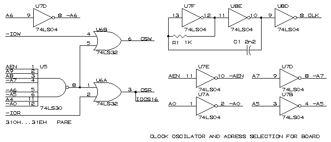
A simple address selection using some TTL circuits ( or better a GAL16V8
device and a programmer, maybe I will write something about this ...) use
the prototype reserved address area. From 310H to 31EH only even address
can be used.
With the same address can be done a 16 bit read (CSR and IOCS16) or a 8 bit
write (CSW) for multiplexing and amplifier devices. A 250KHz oscillator (CLK)
is also presented here.
3. 4 channel multiplexing and variable amplifier stage
Like some " universal devices " K572PV1 can measure only positive or negative input signals. Bipolar signals are a big unknown for this converter. So, I have to do some artifacts to convince converter to work in a bipolar mode:

The four bipolar input signals (max -5V to +5V ) are applied to JP1. If we
have to measure four floated signals (with no common ground) than we use
I1G1, I2G2, I3G3, I4G4 input pins. Eight diodes ( D3 to D10 ) try to protect
the first multiplexing circuit U14 ( but like Murphy said this will protect
the 2Amps fuse from the power supply you apply at JP1...)
Gain of U13 amplifier can be programed from 2 bit ( GAIN1 and GAIN2 ) in
four ranges: x1, x2, x5, x10 . Of course that precision of gain is set from
value of resistors, for a perfect x1.000 gain, variable resistors must be
added. However, a 0.5...1% tolerance resistors is quite acceptable even for
pretentiously... U15 is a summing inverting amplifier, so for a -5V to +5V
input signals ( at JP1 ) the IN signal will be 0V to +10, that means
only 11 bit for measuring and 1bit for sign.
The programming word for multiplexing channels and gain are shown in
next table:
| D3 | D2 | D1 | D0 | GAIN | CHANNEL |
| x | x | 0 | 0 | 1 | x |
| x | x | 0 | 1 | 2 | x |
| x | x | 1 | 0 | 5 | x |
| x | x | 1 | 1 | 10 | x |
| 0 | 0 | x | x | x | 1 |
| 0 | 1 | x | x | x | 2 |
| 1 | 0 | x | x | x | 3 |
| 1 | 1 | x | x | x | 4 |
So, an OUT 310H,xFH means that channel 4 is used with a x10 gain amplifier and a IN 310H, (data) will read a 16 bit word from witch only the last 12 bit are active.
4. Negative reference voltage stage
Well, a serious converter has internal reference, K572PV1
has not... I designed a negative reference using a positive one and a
amplifier because was all I have at that moment:
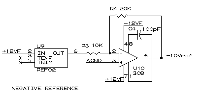
No special comments, external trimming components can be aded, a better way
is to use a -10.24V negative reference
( for example from Maxim...)
5. Miscellaneous ( full schematics, bill of materials, a little C driving program )
This project is only an example for understanding a way for interfacing with
ISA bus. I work a lot at this schematics and
PCB ( made on a protoboard with wire wrapping modified technology) Now there
are a lot of good AD convertors and
full data aquisition chips
(Maxim is
a good example for this) running at high frequencies.
The whole schematics including ISA conector, is here:

A better way for viewing schematics is HP-GL file:
PV1.plt Can be view or
print with Printgl or any other HP-GL viewer.
With the courtesy of
Neamtu
Dorel who write a little
program for driving this board you can have
it from
here. If someone
is interested to built exactly this schematics ( maybe someone from Soviet
Union...) a bill of materials generated
by Orcad4 is also here. That's all folks!
Back to Vasile's
electronics page