We have successfully grown more than 10 typies of Perovskite
Oxide thin |
 |
Homepage-->Research
Atomic engineering of complex oxide thin
film and superlattice by Laser MBE
[Research] [Experience] [Enterprise]
[Interests][Publication]
| 2001,11-now | 1. Optical (sub-minimeter microwave) study of high-Tc superconductors |
| 2. Optical Study of YBCO/LaCaMnO heterostructures and superlattices |
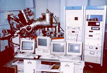
| 1997-2001 | 1. Laser-MBE growth of Complex Oxide thin films and superlattice |
| 2. Surface optical diagnosis and SHG study | |
| 3. Monte Carlo Simulation of the growth kinetics | |
| 4. Oxide heterojunction and High-K dielectric oxide thin film |
1.Laser-MBE growth of Complex Oxide thin films and superlattice
We have successfully grown more than 10 typies of Perovskite
Oxide thin |
|
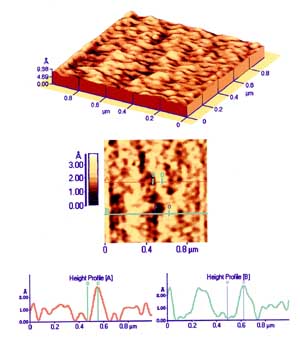 Figure 1 shows an atomic force microscopy (AFM) image of BaTiO3 thin film. The surface root means square roughness is 0.055nm.The height profile suggests that the range is within atomic height 0.2nm. |
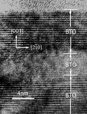 Figure 2 shows a high resolution TEM picture of BaTiO3/SrTiO3 (BTO/STO) superlattice. The thickness of BTO and STO is 20 and 10 unit-cell. It can be clearly counted from this picture. |
||||||||||||||||||||||||||||||||||||
 |
<=== Figure
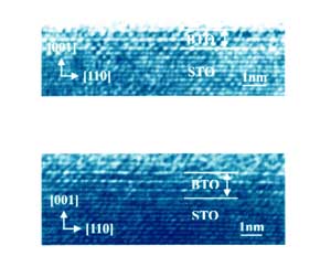
3 Figure 3 shows high resolution TEM picture of ultro thin BaTiO3 thin film on STO substrate. The thickness of BTO is 2 and 3 unit-cell, respectively. |
||||||||||||||||||||||||||||||||||||
| SHG
study of BTO/STO superlattice Paper-Link (pdf)Phys. Rev. B, 60, 1697 Table 1. SHG coefficients of various BTO/STO superlattices with various stacking periodicities
|
The
second-order nonlinear optical susceptibility of [BaTiO3(2 unit cells)/SrTiO3(2
unit cells)]50 Superlattice, d33=156.5pm/V, is 22 times larger than that of bulk BaTiO3
single crystal , d33=6.8pm/V.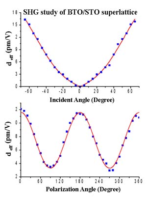 |
2.Surface
optical diagnosis
We adapte an optical oblique-incidence
reflectivity difference (OIRD) device
to the growth chamber of Laser MBE for real-time diagnosis of the growing
surface.[PRB-vol
(57)-page 2514,1998] ;
[PRB-vol
(61)-Page 10404,2000]
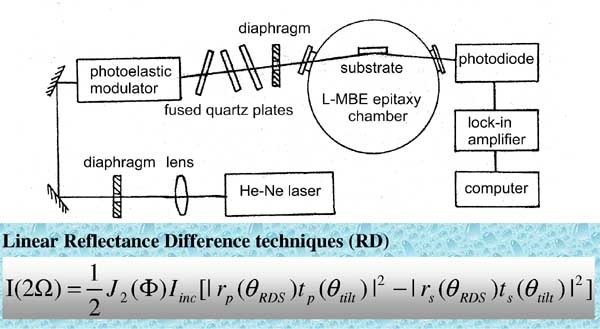 Figure 4 Sketch of the optical setup of the oblique-incidence reflectance difference (OIRD) measurement. PEM: photoelastic modulator. QW: fused quartz parallel plate. PD: biased silicon photodiode. |
|
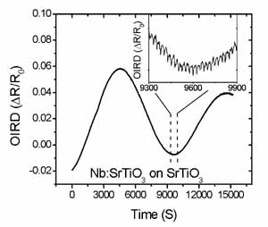 Figure 5 Interference oscillations and monolayer oscillations (the inset) obtained by OIRD during the heteroepitaxy of Nb-doped SrTiO3 on SrTiO3 (100). |
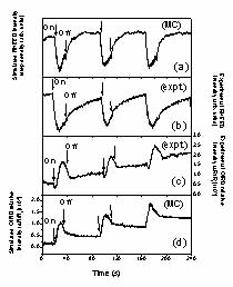
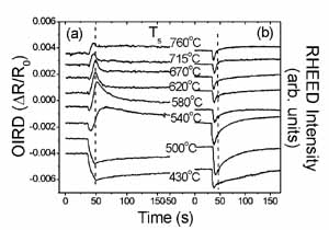 Figure 6 Simultaneously measured OIRD signals (a) and RHEED intensity signals (b) for the growth of one monolayer SrTiO3 as a function of the substrate temperature Ts. The dashed lines indicate the interruption of growth. For more==> |
3. Monte
Carlo Simulation of the growth kinetics
We use Monte Carlo simulation to study the
optical (OIRD) signal and
RHEED response.
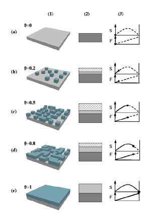 |
<==Figure 7. we treat the topmost incomplete layer as two parts, a surface layer with an average dielectric constant and a film layer below that with the dielectric constant of the bulk film. The variations of the surface layer height during layer-by-layer growth are schematically illustrated in (a)-(e). Column “1” shows the schematic surface morphology for different surface coverage q , column “2” shows the corresponding layer structure in our model. The variations of the surface layer height (S) and the film thickness (F) are shown in column “3”. The dashed curve in column “3” shows the trend of the variations and the solid dot at the end of the solid curve indicates the current value corresponding to the surface morphology shown in column “1”. At the beginning of the deposition on smooth surface, the surface layer height increases as a result of surface roughening (Fig. 7a-7b) and reaches a maximum at about half layer coverage (c). During the subsequence growth, the coalescence of 2D-islands which leads to surface smoothening results in corresponding decrease of the height of the surface layer (d-e). The thickness of the bulk film increases continuously throughout the deposition process. |
Figure 8==> Fresnel’s equations for a multi-layer stack are
used to calculate the reflectivity of s- and p-polarization. |
 |