Metallo-dielectric photonic band gap (MPBG) materials for microwave and millimeter-wave applications
- The photonic band gap (PBG) materials
are artificially fabricated periodic structures that exhibit energy
gaps in which electromagnetic waves of certain frequencies cannot
propagate. The potential applications of PBG materials at microwave
and millimetre-wave frequencies have been realized recently.
> "Metallo-Dielectric Photonic Band Gap (MPBG) Materials for Microwave and Millimeter-Wave Applications " by X. S. Rao, at Temasek Laboratories on 25 May 2002
Related information:
> "Photonic crystals: semiconductors of light" by E. Yablonovitch, Scientific American 285(6), 46-55 (2001)
> Photonic Band Gap Links
> Photonic & Sonic Band-Gap Bibliography
Diluted magnetic semiconductors for spintronics applications
- Spin-based electronics (spintronics),
where both the electron charge and the electron spin are used to carry
information, offers opportunities for a new generation of devices with
enhanced performance. Spintronics applications require materials
combining properties of both ferromagnet and semiconductor. Diluted
magnetic semiconductors (DMS) are alloys of nonmagnetic semiconductor
and magnetic elements. Possible room-temperature ferromagnetism makes
DMS a very promising material for spintronics applications.
Presentations & talks:
> "Towards room-temperature ferromagnetism in Co-doped ZnO thin films" by X. S. Rao, at Centre of Superconducting & Magnetic Materials (CSMM) on 7 October 2002.
Related information:
> "Spintronics" by D. D. Awschalom et al., Scientific American 286(3), 67-73 (2002)
> PhysicsWeb - Spintronics
Ferroelectric thin films for tunable microwave devices
- The dielectric constant of
ferroelectric thin films can be varied through application of an
electric field, which has been used in making electrically tunable
microwave devices. The aim of this work is to improve the microwave
loss and tunability of the ferroelectric films.
> "Pulsed laser deposition of (Ba,Sr)TiO3 thin films for tunable microwave devices" by X. S. Rao, at Temasek Laboratories on 8 May 2002
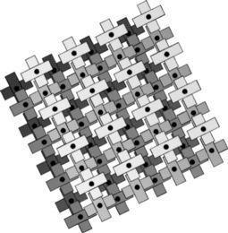
PBG
crystal. Four layers of
the structure form one period of the diamond lattice (from Phys.
Rev. Lett. 80, 2829, 1998).
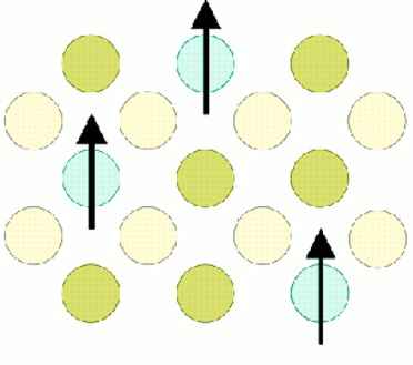
Diluted magnetic semiconductor. An alloy between nonmagnetic semiconductor and magnetic element (from Science 281, 951, 1998)
Experimental Techniques
& facilitiesPulsed laser deposition (PLD)
- A typical PLD system consists of two main parts that can be separated from each other: a deposition chamber and a high-power laser. The former is a vacuum chamber in which a target holder and a substrate holder housed for deposition. The high-power laser enters the chamber through a widow and is used as an energy source to vaporize materials and to deposit thin films. A set of optical components is used to focus and raster the laser beam over the target surface.
- The deposition processes are as follows. A laser beam is focused onto the target surface with an incident angle of around 45 degree. Pulsed lasers are used in order to reach high energy required for ablation. After undergoing complicated beam-solid interactions including energy absorption, surface melting, vaporization of target material and ionization, a plasma region is instantaneously generated near the surface of the target. This plasma expands perpendicularly to the target surface and forms a plume. The plume consists of neutral or ionic atoms, molecules and radicals that then speed toward the substrate. These species reach the substrate with high kinetic energy and are deposited on the substrate surface. As the process is repeated with more laser pulses, a thin film is formed on the substrate surface.
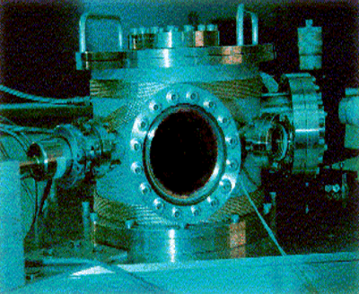
Pulsed laser deposition. One of the most successful vapor deposition techniques in research and device applications.
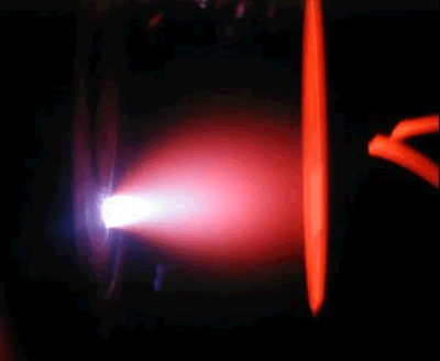
Plasma plume. A plasma generated by laser beam-solid interaction.
home
| resume | research | publications
| links | contact me
Last
Updated: October 16, 2002
by Xue Song Rao