| QuickLinks | Home | GA-586HX | Hot-Swap | AP5T-3 | Q3Test/TNT2 | PA-2012 | H/W-Hack | JiuZhaiGou | Wallpaper |
First off, I must say that this was a crucial step. I couldn't have succeeded without the info I found and the help of some great guys. I searched the Gigabyte newsgroup and found a reference to The Unofficial GA-586HX Homepage set up by Andreas Wohlfeld. This site rocks!! It is the GA-586HX resource on the web, believe me, I searched! I found all the info I needed to hack my GA-586HX here and a whole bunch of helpful enthusiasts. Thanks guys!
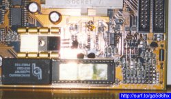
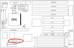
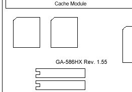
There are many revisions of the GA-586HX. The revision number is printed on the mobo itself. My mobo's revision is 1.55.
The latest official version of BIOS released by Gigabyte is version 2.6. However, version 2.8 was available for a short time on the German Gigabyte Web Site, and was quickly downloaded by some quick thinking guys.
You can get it here 5hx28.zip (141KB).
I flashed the BIOS using this procedure :-
I didn't use Win95 DOS because it's not recommended by Gigabyte. I used the af535a.exe instead of the latest awdflash.exe because it's recommended by Gigabyte for older mobos. The command I used automatically saved the existing BIOS into a "oldbios.bin" file and flashed the new BIOS.
4. Set the clock multiplier and bus frequency
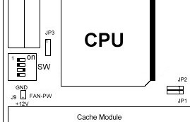
The clock multiplier is controlled by dip-switches SW1 and SW2. The bus frequency is controlled by SW3 and SW4. All 4 are in the dip-switch block SW. Note that some revisions of GA-586HX do not have SW, instead they use JP3 and JP1-2 respectively.

Unmodified, the SW1 and SW2 can only give a maximum of 3x multiplier. This was okay for older CPUs like the Cyrix P166+ because they only required 2 switches to control their BF0 and BF1 pins. BF0 and BF1 are the control inputs that determine the clock multiplier the CPU uses. Newer CPUs like the K6-2 have a new 3rd pin called BF2.
This table shows the clock multiplier settings :-
| K6-2 Clock Multiplier | BF0 | BF1 | BF2 | SW1 | SW2 | JP3(1-2) | JP3(3-4) |
| 4.5 | 0 | 0 | 0 | ON | ON | Close | Close |
| 4.0 | 0 | 1 | 0 | ON | OFF | Close | Open |
| 5.0 | 1 | 0 | 0 | OFF | ON | Open | Close |
| 5.5 | 1 | 1 | 0 | OFF | OFF | Open | Open |
| 2.5 | 0 | 0 | 1 | ON | ON | Close | Close |
| 2.0/6.0 | 0 | 1 | 1 | ON | OFF | Close | Open |
| 3.0 | 1 | 0 | 1 | OFF | ON | Open | Close |
| 3.5 | 1 | 1 | 1 | OFF | OFF | Open | Open |
This table shows the bus frequency settings :-
| Bus Freq | SW3 | SW4 | JP1 | JP2 |
| 50MHz | ON | ON | 1-2 | 1-2 |
| 60MHz | OFF | ON | 1-2 | 2-3 |
| 66MHz | ON | OFF | 2-3 | 1-2 |
| 55MHz | OFF | OFF | 2-3 | 2-3 |
I needed a multiplier of 5.5. From the table, SW1=OFF and SW2=OFF. For 66MHz bus frequency, I set SW3=ON and SW4=OFF. This gives 366Mhz or 5.5 x 66.
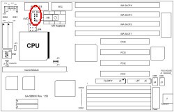
As you can guess from the clock multiplier settings table, BF2 must be set to 0 or grounded in order to achieve 4.0x - 5.5x. To do this, I inserted a short (1cm) and thin piece of "wire-wrapping" wire into the W35 and V36 holes of the CPU socket. This is shown by the red line in the diagram below. You can find the required holes easily by counting 9 holes down the left-most column of holes and inserting the wire into the adjacent holes of the 2nd and 3rd columns, as shown in this diagram.

6. Disable auto-voltage detection
To get 2.2v core voltage which is required by the K6-2, I disabled the auto-voltage detection mechanism. This involved removing 2 small chips from the mobo and jumpering JP4. In the diagram below, the 2 small chips removed are marked by 2 red Xs, and JP4 was jumpered as shown by the red lines.


This is what it looks like. Not a pretty sight, huh? I fairly ripped the 2 chips off my mobo!
Disabling auto-voltage detection is just the 1st step to getting 2.2v. The 2nd step is to modify the actual voltage being supplied by the voltage regulator (VR). This involves soldering additional resistors onto the mobo.

To make things simple (relatively), the core voltage supplied by the VR is determined by this formula :-
Vo = Vref (1 + R1/R2), where
Hence to get Vo = 2.2v, I modified R1 to be about 78W. I did this by adding two 100W resistors to Rm. Since Rm is in parallel with R1 and Rm // R1 = 200W // 130W = ~78W, this effectively makes R1 = 78W.
This is what it looks like. One end of each resistor is soldered onto a solder pad and then other ends are jumpered together.
Measurement of the core voltage required 4 things; 3 100W resistors and 1 multimeter. I removed the CPU, inserted the 3 resistors are shown in the diagram, and locked the socket lever. I removed all cards and RAM from the mobo, and connected the power supply. After switching it on, I measured the core and I/O voltages across their respective 100W resistors with the multimeter. The results were as I expected.
Core Voltage = 2.23v
I/O Voltage = 3.38v

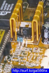
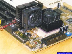
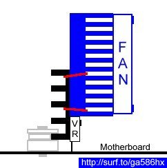
9. Enhance the voltage regulator heatsink
The AS2880 voltage regulator and its heatsink were never meant to support the K6-2. New CPUs like the K6-2 require more electrical current than older ones like the Cyrix P166+. As such, the VR and heatsink get very very very hot when trying to supply current to the K6-2.
To prevent the VR from overheating and dying on me, I replaced its heatsink with a heatsink/fan combo. This heatsink/fan is meant for CPUs, but I found it works fine in cooling the VR. I unscrewed the VR from the mobo and removed the original heatsink. I straightened the VR's 3 legs so that it stood vertically. I then screwed it to another bigger VR heatsink (which was salvaged from an old and dead mobo), and attached the heatsink/fan to the VR heatsink with some metal clips scavenged from clothes pegs. the whole assembly was screwed onto the mobo with 2 plastic and 1 metal washers for support. I applied some heatsink compound (that not-so-white sticky stuff ;^) ) where the VR, VR heatsink and heatsink/fan are in contact. This is to ensure good thermal contact and heat transfer. This diagram shows the side view.
This is what it looks like.
Why did I design the enhanced VR heatsink that way?
10. Cross 'em fingers and boot 'er up!
Upon bootup, the BIOS detected my CPU as a AMD K6 3D running at 366MHz. This is okay because "AMD K6 3D" was the original name for the K6-2. The system started and entered Win95 without problems. So far so good. Btw, I used a "clean" copy of Win95 with only ZD Winstone 98 installed.
I ran the Winstone 98 benchmark once and touched the VR and heatsink. The VR was hot, but not too hot. I could keep my finger on it for 5 seconds without feeling any pain. The heatsink was warm. To make sure the modified heatsink was doing a good job of conducting heat away from the VR, I switched off the fan and touched the heatsink again. This time it was hot, almost as hot as the VR. So I was certain that my modified heatsink was working.
To test the entire system stability, I ran Winstone 98 again, but this time in "demo" mode. This mode runs thru the benchmark, reboots and then starts all over again. I ran it this way for more than 4 hours.
It worked fine!! :)
11. Notes
| QuickLinks | Home | GA-586HX | Hot-Swap | AP5T-3 | Q3Test/TNT2 | PA-2012 | H/W-Hack | JiuZhaiGou | Wallpaper |