
The Schematic view allows you to design and see the standard cell on the transistor level. Similarly Symbol view will allow you to make and see the symbol of the logic device.
1. To create a Schematic view. Start from the library manager and highlight the library in which you want to create the new cell. In this case we have chosen: std_cells_hp05um, then go: file >> new >> cell view

2. Now you must select the cell name and view name. The cell name will most likely incorporate the logic type and other important information such as the capacitive load it will be expected to handle, for this example we have chosen sample_and_lp_4x, since it is an AND type gate, lp for low power and 4x since it will drive 4 times the unit load capacitance, in our case .1pF. View name should reflect the type of view it is, in our case schematic. Be sure to change the tool to Composer-Schematic.

3. Now hit OK, and a new window will launch. You are now ready to begin a new standard cell!
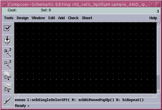
4. Once in the Composer-Schematic view, on the left hand side will be column of buttons. From there you will be able to add all the components need to create the standard cell. For this example we will create a AND gate. First we will add the transistors. Click the "Component" button.
![]()
Then you will get this window:
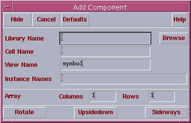
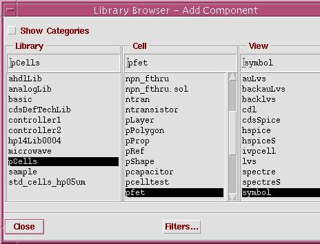
Click Browse, then this window will appear. Select pCells and if you want to add a transistor, select pfet and the symbol view. The pCells file is available for download from the Digital Standard Cell page.
Now drag the cursor back over the schematic view and the image of a PMOS transistor will appear, click once to place the transistor on the sheet.

Now do the same for the NMOS transistors

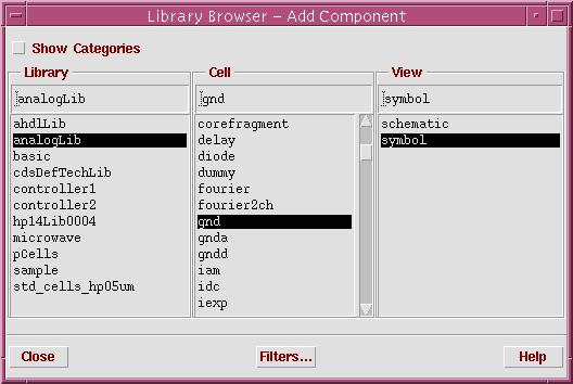
We will also need to add Vdd, Gnd (ground) and input and output Pins. Vdd and Gnd are located in the analogLib library
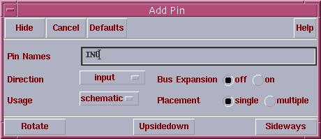
5. To add input and output pins click on the Pins button:
![]()
Then this window will open, Name the pin and make sure to define if it is an output or input pin. Again place these pins on the diagram.

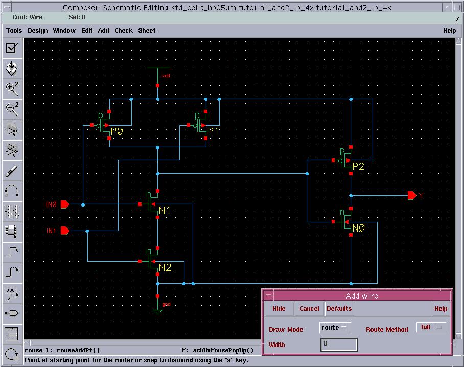
6. Now that we have put all the components in the schematic view, it's time to connect them. Select the thin wire button.
![]()
Now wire everything up correctly. We can hit the "s" button for the wire to attach itself to the nearest terminal. So now our schematic should look like this.
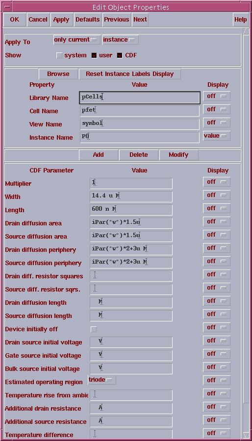
7. Finally we need to size the transistors. To do this we highlight the transistor we want to size and then hit the property button.
![]()
Then you will be able to select the length and width. The Length is fixed but the width will need to be determined depending on the transistor layout in the standard cell.
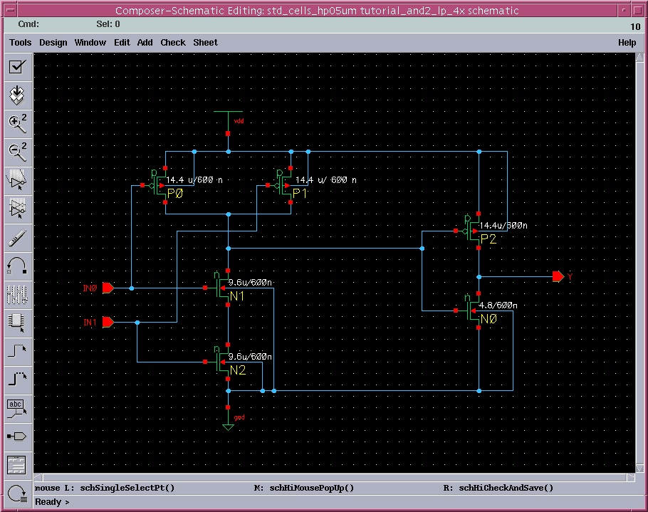
Once all the transistors have been sized, you schematic should look something like this.
Cadence is a trademark of Cadence Design Systems, Inc., 555 River Oaks Parkway, San Jose, CA 95134
Synopsys is a trademark of Synopsys Inc, 700 East Middlefield Rd. Mountain View, CA 94043